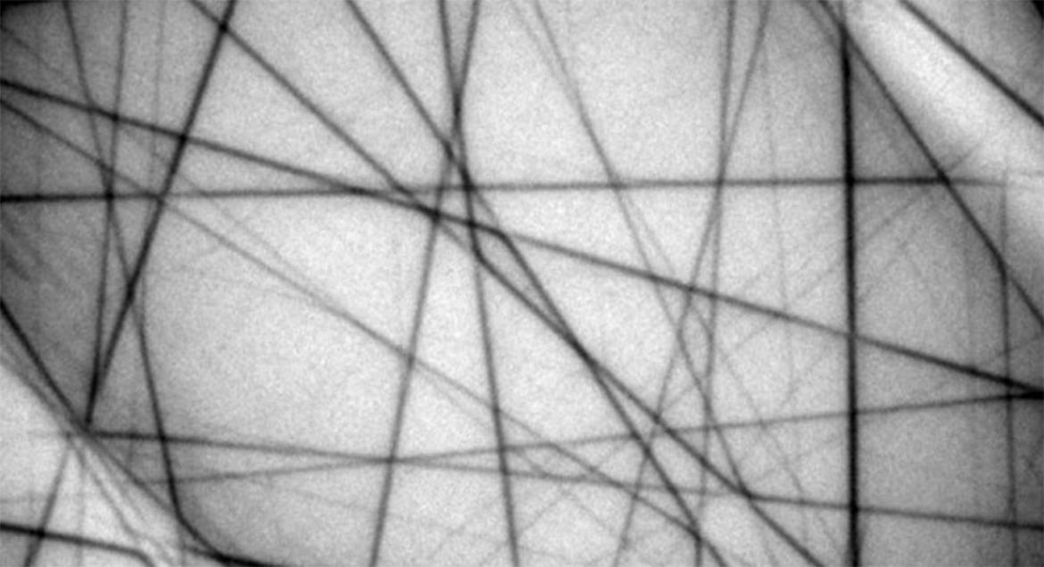
The mechanical strain in crystals affects their physical, electronic, optical and magnetic properties. In micro- and nano-electronic industry, the study of strain accumulated during the technological processes in device definitions has been of great interest to monitor the generation and evolution of crystal defects [1]. More recently, the controlled generation of crystal strain is used to tailor the mobility of carriers in bandgap engineering, such as in SiGe structures [2] or the opto-electronic properties of semiconductors, e.g. in strained silicon waveguides [3].
The Convergent Beam Electron Diffraction (CBED) method in the Transmission Electron Microscope is an established technique capable of yielding quantitative strain information in crystals, with a spatial resolution at the nanometer scale together with a strain resolution of the order of 10‑4. Basically, it is point-to-point technique based on the analysis of the strain induced shift of High Order Laue Zones (HOLZ) deficiency lines, which occur in the central disk of a convergent-beam electron diffraction pattern, taken in a zone axis where the HOLZ lines are free from dynamical interactions. The Bologna section of IMM has implemented such technique in a Scanning Transmission Electron Microscopy (STEM) [4] and developed a dedicated routine for the analysis and extraction of the strain tensor values from the diffraction patterns, based on quasi-kinematical simulations of electron diffraction [5]. The strain analysis can be performed in Si based devices and structures, such as STI structures, although it can be virtually extended to any ordered, crystalline material.
The CBED technique can also be used to monitor the quality of the crystal, i.e. measure the disorder in the structure atomic arrangement [6]. In addition the conventional CBED technique for strain analysis, the Large Angle CBED (LACBED) method can be used to directly monitor strain in an image where spatial and diffraction information are superimposed [7]. While in the LACBED method the strain detection is straightforward, the extraction of quantitative information requires dynamical simulations [8].
[1] V. Senez, A. Armigliato, I. De Wolf, G. Carnevale, R. Balboni, S. Frabboni, A. Benedetti, J. Appl. Phys. 94, 5574-5583 (2003).
[2] F.Schaeffler, Semicond.Sci.Technol.12(1997)1515.
[3] [2] M. Cazzanelli, F. Bianco, E. Borga, G. Pucker, M. Ghulinyan, E. Degoli, E. Luppi, V. Véniard, S. Ossicini, D. Modotto, S. Wabnitz, R. Pierobon, L. Pavesi, Nature Mat. 11, 148-154 (2012).
[4] A. Armigliato, R. Balboni, A. Benedetti, and S. Frabboni, Analysis of localised strains by Convergent Beam Electron Diffraction in ‘High-pressure crystallography, Eds A. Katrusiak and P. McMillan, ISBN 10: 140201953X, 1402019548, Kluwer Academic Publishers, Dordrecht, 2004, pp. 277-294.
[5] Deliverable D2, STREAM project, p.25 (2000) (http://stream.bo.cnr.it/docs/pdocs.html)
[6] S. Frabboni, F.Gambetta, A.Armigliato, R.Balboni, S.Balboni, F.Cembali, Physical Review B 60 (19) (1999) 13750–13761.
[7] F. Wu, A. Armigliato, R. Balboni and S. Frabboni, Ultramicroscopy 80,(1999), 193-201.
[8] A. Spessot, S. Frabboni, R. Balboni, and A. Armigliato, Journal Of Microscopy-Oxford, Volume 226, Issue 2, 140-155, 2007.


