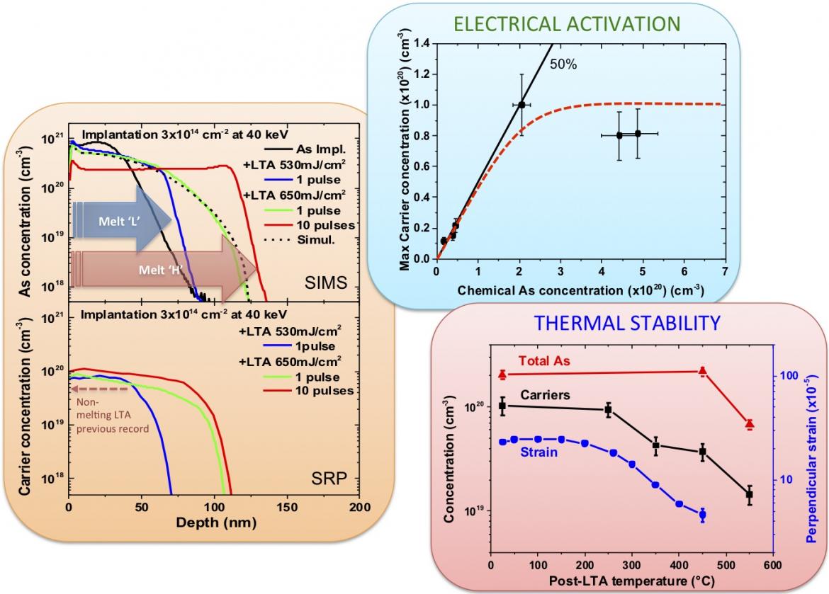
Germanium is experiencing a renaissance during the last decade for several advanced applications such as high- mobility non-Si CMOS transistors to overcome the limits of Si scaling, infrared photodetectors, infrared-emitting lasers based on Ge, mid-infrared plasmonics based on heavily doped Ge, etc. However, high doping of Ge poses several issues due to the limited equilibrium dopant solubilities and detrimental dopant-defect interactions.
This activity aims at overcoming the above limits by exploiting pulsed laser thermal annealing (LTA) processes in the melting regime. Thanks to the highly non-equilibrium nature of this technique, some promising results have already been reported in literature, also by CNR-IMM researches, demonstrating high dopant activation levels in Ge with good control of dopant diffusion.
This activity aims at investigating and modeling the basic mechanisms involving the atomic transport and defect generation during LTA in Ge, and to investigate the diffusion, activation and interaction with impurities or defects of different dopants such as P, As, Al and Ga both during LTA and during post-LTA conventional annealings.
Our goal is to achieve a better understanding and to produce junctions in Ge with unprecedented high activation levels, shallow junction depth, high control of impurity and defect concentrations. This should facilitate the realization of future advanced microelectronic and photonic devices based on Ge.

