
Research field
Future society faces a major challenge: finding a sustainable balance between limited natural resources and the growing need for energy, materials, connections between people...
Nowadays, micro-nanoelectronic research addresses on one side the continuous scaling of logic and memory devices, also in view of targeting low power electronics and new functionalities. These objectives have been achieved by introducing new materials, exploiting new physical mechanisms and innovative fabrication methods, and with the support of modeling, simulation and design tools. On the other side, there is an increased interest to develop new systems and new computing paradigms, which can address the current emerging societal challenges. For instance, the yearly increasing amount of generated data and the Internet of Thing applications demands for more efficient computation systems in terms of power and capability, to solve problems where the standard von-Neumann based platform fails.
In this framework, the CNR-IMM Institute has a long term and internationally recognized experience in the field of materials, technologies and simulation of logic and non-volatile memory devices. More recently, the Institute has also gained a recognized expertise in developing devices and simulations for neuromorphic and quantum computation paradigms. The institute is currently at the forefront of emerging technologies in the above fields, and the research activities are carried out in collaboration with leading Industries in the field, as well as Italian/international Universities and Research Centers.
The research activities are carried out in different Units of IMM (Agrate Brianza, Bologna, Catania Unit, Catania Headquarters) and are currently focused on the following macro-areas:
Coordinator: Spiga Sabina

Research field
Future society faces a major challenge: finding a sustainable balance between limited natural resources and the growing need for energy, materials, connections between people...
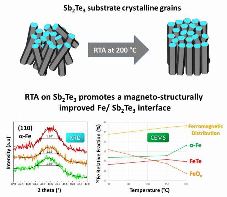
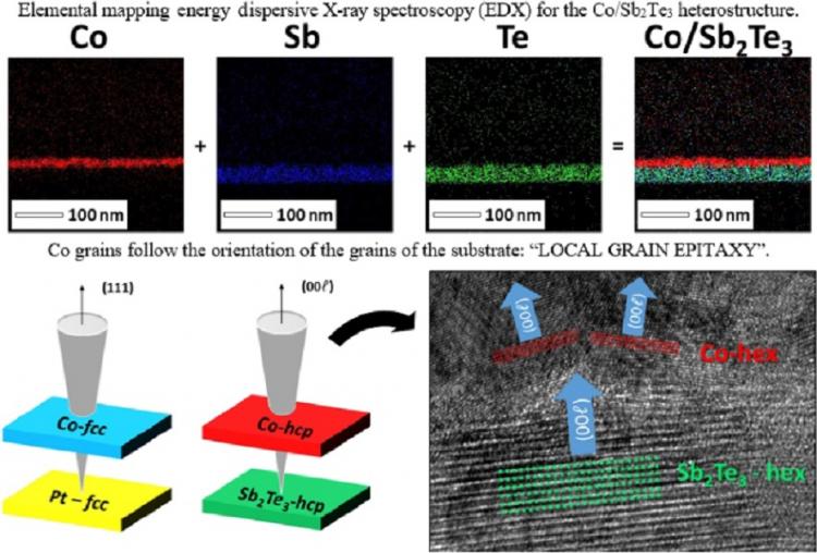
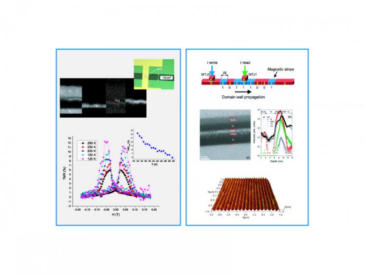
Topological insulators are in the focus for enhancing spin‐to‐charge conversions when in contact with ferromagnets, and to optimize the interface is demanding. In our paper published in Advanced...
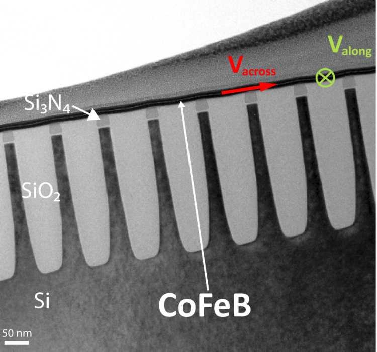
Controlling the motion of magnetic domain walls (DWs) in ultrathin films with perpendicular magnetic anisotropy (PMA) has opened perspectives for mass-storage applications such as “racetrack...
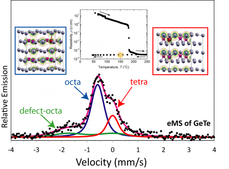
The unique method of 57Fe emission Mössbauer spectroscopy (eMS), as performed at the large-scale facility of ISOLDE at CERN, was employed to reveal, at the most atomic-scale,...
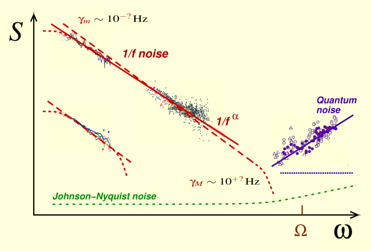
Developing Quantum Technologies (QT) requires protection of coherence and quantum correlations, as entanglement, from effects of the environmental noise due to uncontrolled degrees of freedom....
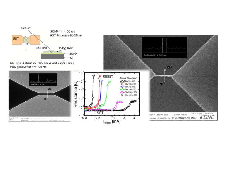
Giuseppe D'Arrigo, CNR-IMM Catania
The working principle of a Phase Change Memory (PCM) cell exploits the reversible...
Germanium is experiencing a renaissance during the last decade for several advanced applications such as high- mobility non-Si CMOS transistors to overcome the limits of Si scaling, infrared...
This research activity at IMM Agrate is mainly focused on the use of chemical methods such as atomic layer deposition (ALD) and chemical vapour deposition (CVD) to synthesize materials for...
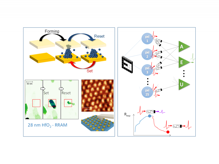
Memristive systems represent today a disruptive technology for the semiconductor industry towards several applications such as data storage (non-volatile memories), non-volatile...