| MORPHOLOGICAL, STRUCTURAL AND CHEMICAL CHARACTERIZATION |
|
|
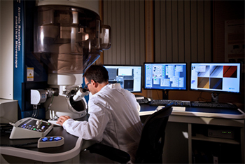
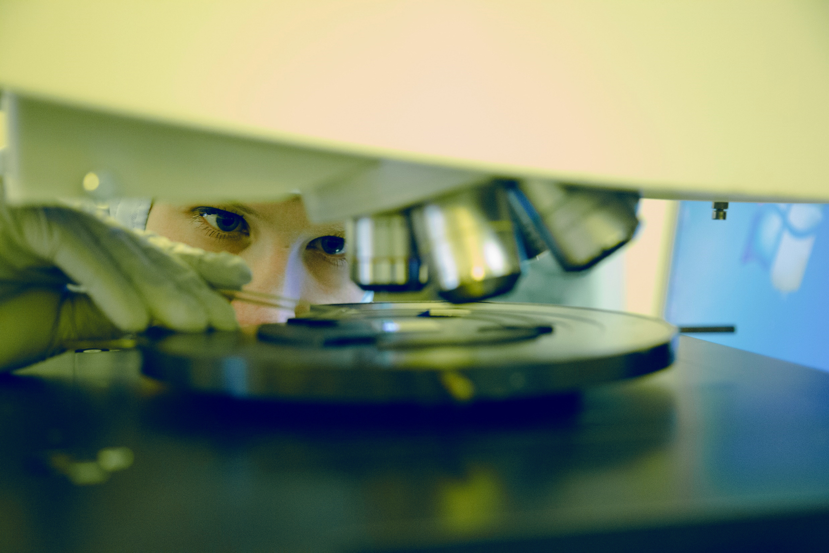
Electron microscopes
- Transmission Electron Microscopy (TEM, HRTEM) CHQ, B, L
- Scanning Electron Microscopy (SEM, environmental SEM) CHQ, C, A, B, L, R
- Scanning Transmission Electron Microscopy w/o aberration correction (STEM) CHQ, B
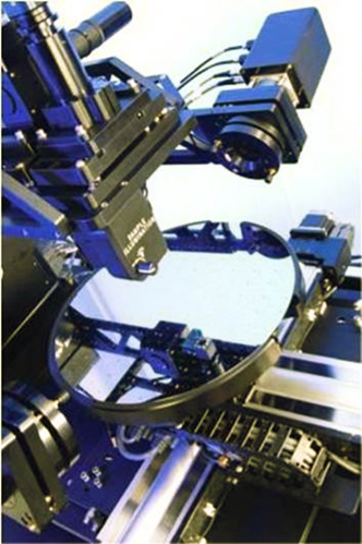
- Dual Beam Microscopy (FIB-SEM) CHQ, B, L
Scanning probes
- Atomic Force Microscopy (AFM, MicroRaman/TERS integrated) CHQ, C, A, L, R
- Scanning Tunneling Microscopy (STM) A, R
X-rays methods
- X-Ray Diffaction (XRD) CHQ, A, B, R and X-Ray Reflectometry (XRR) A, B
- X-Ray Photoelectron Spectroscopy (XPS, ESCA) A
- X-Ray Fluorescence (XRF) A, R
Hyperfine structure methods
- Electron Paramagnetic Resonance (EPR) A
- 57Fe and 119Sn Conversion electron Mössbauer spectroscopy (CEMS) A
- On-line Mössbauer spectroscopy @ ISOLDE-CERN A
Chemical methods
- Time-of-Flight Secondary Ion Mass Spectrometry (ToF-SIMS) A
- Total Organic Carbon Analyser C
- Micro-Photoluminescence CHQ, L
- Fourier Transform Infrared Spectroscopy (FTIR) R, A
- Gas sensor characterization B, L, R
- Chemical Analytical methods by Gas Chromatography/Mass Spectrometry (GC/MS) L
- Chemical Analytical methods by Gas Chromatography/Flame Ionization and Pulsed Discharge Detector (GC/FID and GC/PDD) B
- IR Spectrophotometry C
Optical methods
- Ellipsometry CHQ, A
- E-Line HR EBL CHQ
- Raman Microscopy-TERS CHQ, R, L
- Optical Microscopy CHQ, L
Other methods
- Contact Angle measurement system C
- BET surface area analyser C
- Scanning Microwave Microscopy R
- TDS-THZ Imaging R
|
| ELECTRICAL, ELECTRO-CHEMICAL AND MAGNETO-ELECTRICAL CHARACTERIZATION |
 |
Scanning probes and electron microscopy based methods
- Kelvin Probe Force Microscopy (KPFM) A L
- Conductive Atomic Force Microscopy (C-AFM) CHQ, C, A, R, L
- Magnetic Force Microscopy (MFM) A, L
- Electrostatic Force Microscopy (EFM) A, R, L
- Scanning Electron Microscopy-Cathodoluminescence C
- In-situ TEM under electrical and chemical stimuli B
- In-situ TEM/STEM under optical stimuli CHQ
Electrical methods
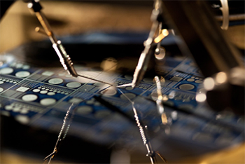
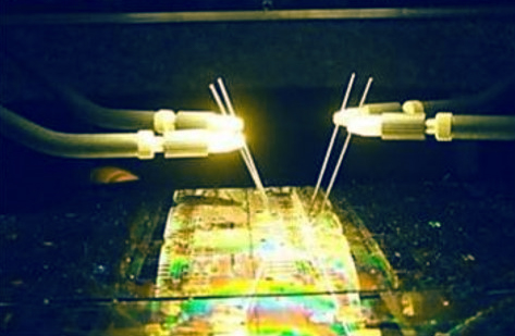
- Probe-Stations for AC/DC/pulsed measurements CHQ, A, B, L, R
- Probe for thin films piezoelectric characterization R
- Impedence analyzer L, R
- Electrodynamic Skaker R, L
- PAR-apparatus CHQ
- Four points sheet resistance CHQ
- Spreading Resistance Probe CHQ
- Piezometer L
- Electrical Impedance Spectroscopy with LCR Meter L
- Deep-level transient spectroscopy (DLTS) CHQ
Electro-chemical methods
- Low current electrochemical characterization in solution and solid-state B
- Electrochemical impedance spectroscopy B
- Photo-electrochemical characterization B
- Potentiometry C, R
Electro-optical methods
- Electro-optical characterization CHQ, L
- Internal Photoemission Spectroscopy (IPE) A
- Setup for spectral photocurrent and photocurrent mapping L
- Setup for deep levels and current dynamics characterization L
- Setup for optically induced electrical pulses in lipidic membranes L
Magneto-electrical methods
- Magnetotransport Facility (Magnetoresistance) A
- Quantum transport (Criomagnet @ He temperature) A
- Ferromagnetic Resonance (FMR) w/o Vector network analyser R
- Hall Effect Measurement System CHQ, A, B, L
|
| OPTICAL CHARACTERIZATION |

 |
Raman
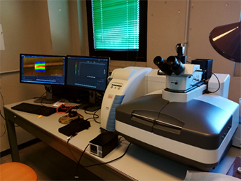
- Micro-Raman spectroscopy (multi wavelength, vis UV, thermal stage) CHQ, A, R, L
- Confocal Optical Microscope for microPL and microRaman 2D Mapping- Fluorescence Lifetime Imaging (FLIM) L
- Integrated AFM-MicroRaman-TERS system L
Infrared, visible, UV
- Fourier-Transformed Infrared Spectroscopy (FTIR) A, R, B
- IR Spectrophotometry C
- Ultraviolet-Visible-near Infrared Spectrophotometry (UV-Vis-NIR) C, A, B, L, R
- Spectroscopic Ellipsometry (SE) A
- CW and ps-ns Photoluminescence (Time resolved) C, L, R
- Spectrofluorimetry L
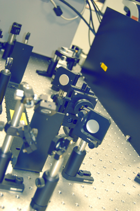
- Lasers CHQ, L
- UV-LED Lamp C
- Photo/Electro-Reflectance L
- Photocurrent spectroscopy L
- Electroluminescence C, L
Other methods
- Optical/Polarization Microscopy R
- Near-Field Microscopy R
- Photovoltaic lab CHQ
- Solar Cell Characterization/Simulator CHQ, C, B
- Streak camera for 1 ps Time Resoved Spectroscopy L
- Electro-optical setup based on Pockels effect L
- Plasmon enhanced fluorescence spectroscopy (PEF) L
- TMOKE Magneto-optical characterization (multiwavelength VIS and variable angle configuration) L
- SPR and LSPR in Krestchamn configuration L
- Optical fiber – integrated Nanoplasmonic characterization L
- Laser doppler vibrometer B
- Characterization of the frequency response of optical devices B
- Characterization of the polarization of optical signals B
- 12 GHz and 150 MHz band optical characterization B
|
| THERMAL CHARACTERIZATION |
 |
- Raman Thermography R
- 3-omega van der Pauw thermal resistivity A
- In-situ TEM under thermal stress, B
- In-situ TEM/STEM under cryogenic temperature CHQ
|
| SPECTROSCOPIES |
 |
- Micro-Raman spectroscopy (multi wavelength vis UV, thermal stage) A, R
- Fourier-Transformed Infrared Spectroscopy (FTIR) A, B, R
- Ultraviolet-Visible-near Infrared Spectrophotometry (UV-Vis-NIR) C, A, B, R
- Spectroscopic Ellipsometry (SE) A
- Internal Photoemission Spectroscopy (IPE) A
- 57Fe and 119Sn Conversion electron Mössbauer spectroscopy (CEMS) A
- On-line Mössbauer spectroscopy @ ISOLDE-CERN A
- IR Spectrophotometry C
- Scanning Microwave Microscopy R
- Terahertz time-domain (TDS-THZ) Spectroscopy/Imaging R
- Transient Absorption Spectroscopy R
- CW and ps-ns Time Resolved Photoluminesce L, R
- Electron Energy Loss Spectroscopy CHQ
- Photo/Electro-Reflectance L
- Photocurrent spectroscopy L
- Confocal Optical Microscope for microPL and microRaman 2D Mapping- Fluorescence Lifetime Imaging (FLIM) L
- Streak camera for 1 ps Time Resolved Spectroscopy L
- Gas chromatography coupled to mass spectrometer (MS) and gas sensor L
- TEM/STEM-Energy Dispersive X-Ray Spectroscopy CHQ, L
- TEM/STEM-Electron Energy Loss Spectroscopy CHQ, L
|
