
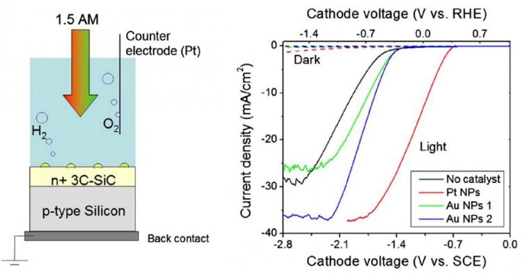
At IMM-CNR Catania we use the plasmonic properties of noble metal nanoparticles (Au or Pt) to improve the photo-electro catalytic activity of n-type 3C-SiC/p-type Si heterojunction solar cells, to...
Optoelectronic, Plasmonic and Photonic Devices
Silicon photonics and hybrid integration optoelectronic technologies are incredibly pushing industrial research that looks forward to the effective and low cost integration of absorption-free optical components and micro/nanoelectronic circuits on the same chip. The Institute is strongly involved in this field, focusing the research on the main goals of i) overcoming the silicon intrinsic inability to emit light, ii) developing new families of photodetectors, and iii) discovering original light manipulation techniques on chip at a sub-micron scale. The studied devices and technologies are thought for on-chip and intra-chip optical interconnects, future optical networks for ultrafast data transmission, and optical-based micro/nanosystems.
A strong interest is in perspective devoted to the quantum technologies, and in particular to the design of quantum hardware and software. The activities are based on the solid Institute know how in the realization of micro and nanophotonic devices which can find direct application to the development of quantum integrated circuits and systems.
Nanophotonic biological structures, such as diatoms, are also studied to exploit their unique properties in the design and fabrication of new bio-inspired devices and biomimetic optoelectronic systems, such as super-lenses and solar concentrators.
Moreover, photonic technologies are exploited for the realization of innovative imaging and spectroscopy systems. They are mainly based on digital holography, linear and nonlinear raman effects, interferometric and spectroscopic technologies. The applications are in label free imaging and microscopy in biomedicine, in material science, in micro/nanoelectronics, and in several fields of preeminent industrial interest.
Finally, fiber optic devices and systems exploiting new concepts, such as plasmonic structures and metasurfaces on-the-fiber-tip, are developed for the realization of innovative optical biochemical and physical sensors, paving the way to lab-on-fibers systems.
A permanent staff of more than 60 researchers from the different Institute sites is involved in the Optoelectronic activities, which can be mainly related to the following topics:
- Silicon photonics for ICT and optical interconnects
- Rare-earth doped Si-based materials for photonics and lightning
- Development of SPAD detector and photomultipliers
- Light detectors based on Si, Ge and ZnO nanostructures
- Nanophotonics with metamaterials, plasmonic and photonic crystal structures
- Optoelectronic components based on reduced dimensionality structures and microcavities
- Quantum technologies
- Natural photonic structures and biomimetics
- Development of innovative optical methods for label free interferometric imaging
- Volume holographic optical elements: design and possible applications
- Nonlinear microscopy and bioimaging based on stimulated Raman scattering
- Optical spectroscopy of semiconductor nanostructures
- Fiber optic sensors and lab-on-fibers systems
Coordinator: Giorgia Franzò
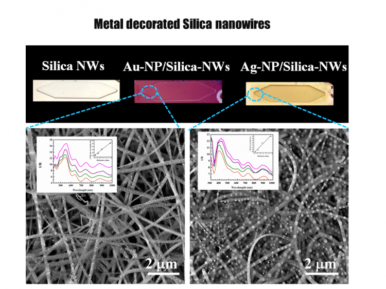
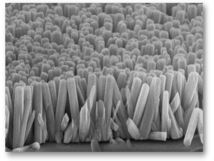
Highly disordered (forest) SiO2 nanowires (NWs), obtained by oxidizing SiNWs, have been decorated with metal (Au, Ag) nanoparticles (NPs). These hybrid structures combine strong scattering...
Many efforts of the scientific community working in the field of nanophotonics are currently devoted towards the development of a Si-based light source able to be used for the...
One of the bottlenecks for the widespread application of Si photonics, and for the merging of electronic and optical functions on the same chip, is the lack of efficient light...
Light detection will be attempted by using Si and Ge quantum structures embedded in insulating matrices or by low-cost synthesized ZnO nanostructures.
The first activity is focused on the...
Team: Salvatore Lombardo, Sebania Libertino, Stefania Privitera, CNR-IMM, Catania
The Silicon Single Photon Avalanche Detectors (SPADs) and the Silicon Photomultipliers (...