
Synthesis and Micro/Nano Fabrication
| The Micro- and nano fabrication (MNF) network has the capacity to produce excellent scientific research and has the potential to support the various research activities starting from basic research up to applied research with high TRL. | |
 |
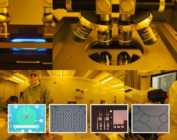
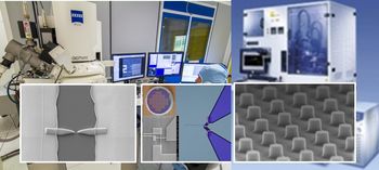
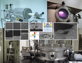
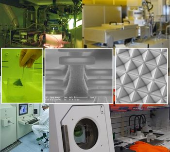
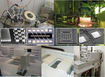
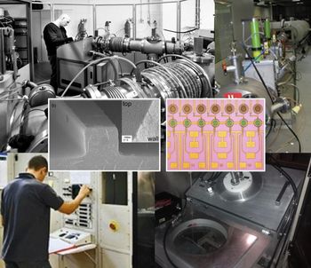
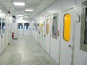
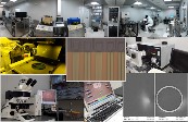
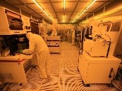
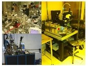
The MNF-network has necessary expertise and state-of-the-art technological facilities (about 1400 m3 ISO 5-8 Clean Room and more than 170 equipment) distributed over 7 sites in Italy able to investigate and develope a wide set of processes covering the whole chain for the fabrication of
The network also has a strong application connotation, and is potentially capable of favoring and encouraging technology transfer to small, medium and large companies both in Italy and abroad. It is also able to support small and medium production. MNF network is inside the Italian network of research infrastructures in the field of nanofabrication (It-Fab). |
COORDINATOR: RITA RIZZOLI
| OPTICAL AND LASER LITHOGRAPHY | |
 |
For more details see the following links |
| NANOLITHOGRAPHY AND NANOPROCESSING | |
 |
For more details see the following links |
| GROWTH, DEPOSITION AND THERMAL PROCESSES | |
 |
For more details see the following links |
| WET AND DRY ETCHING | |
 |
For more details see the following links |
| MICROSYSTEM PROCESSES | |
 |
For more details see the following links |
| ION IMPLANTATION | |
 |
For more details see the following links |
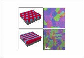
| METROLOGY, CONTROL AND ELECTRICAL CHARACTERIZATION | |
 |
For more details see the following links |
| PACKAGING | |
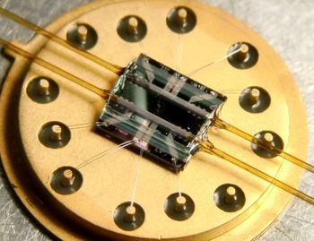 |
For more details see the following links |
| SIMULATION AND DESIGN | |
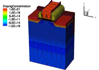 |
For more details see the following links |
 |
 |
 |
 |
| AGRATE UNIT | BOLOGNA UNIT | ROME UNIT | NAPLES UNIT |
 |
 |
 |
|
| LECCE UNIT | CATANIA HQ UNIT | CATANIA UNIT |