
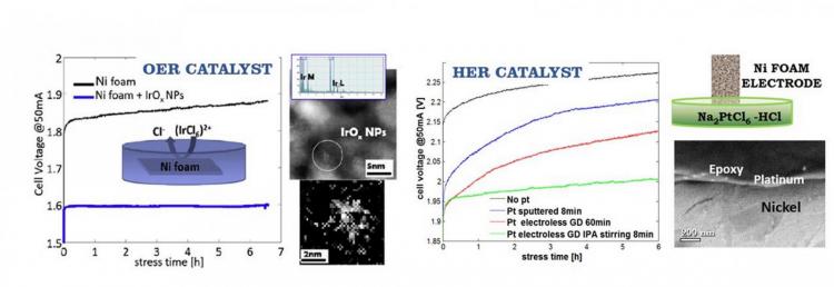
The realization of electrochemical cells for the synthesis of green fuels, such as hydrogen, by water splitting, or ammonia by reaction of nitrogen gas with water or green hydrogen, represents an...
MOEMS and Multifunctional Systems
MEMS (Micro-Electro-Mechanical System) and MOEMS (Micro-Opto-Electro-Mechanical System) devices can be designed to be employed in a wide range of applications. They commonly involve micromachining techniques in their fabrication and may operate exploiting mechanical, thermal, electromagnetic and optical principles.
IMM institute possesses an established know-how related to the design, manufacturing and characterization of MEMS and MOEMS devices, including:
- Fabrication and characterization of MEMS for microwave and millimeter wave communication, such as switches, electromagnetic resonators, micro and nano-antennas on Si, Al2O3, SiC e GaAs substrates.
- Integration of innovative functional materials for piezoelectric, thermoelectric and chemical transduction produced with advanced synthesis techniques like Atomic Layer Deposition (ALD) and Metal-Organic Chemical Vapour Deposition (MOCVD) in MEMS.
- SiC MOEMS for pressure sensing within the cylinders of internal combustion engines.
- Fiber-optic ultrasonic probes manufactured by MOEMS technology for minimally invasive medical diagnostics.
- MEMS for micro-energy harvesting from heat sources based on semiconductor nanowires manufactured by top-down technology.
- MEMS physical sensors suited to be used on automated equipments (resonant strain sensors, absolute pressure sensors, inertial and acoustic sensors for vibrations).
- Innovative MEMS/NEMS (Nano-Electro-Mechanical Systems) based on two-dimensional materials (graphene, MoS2).
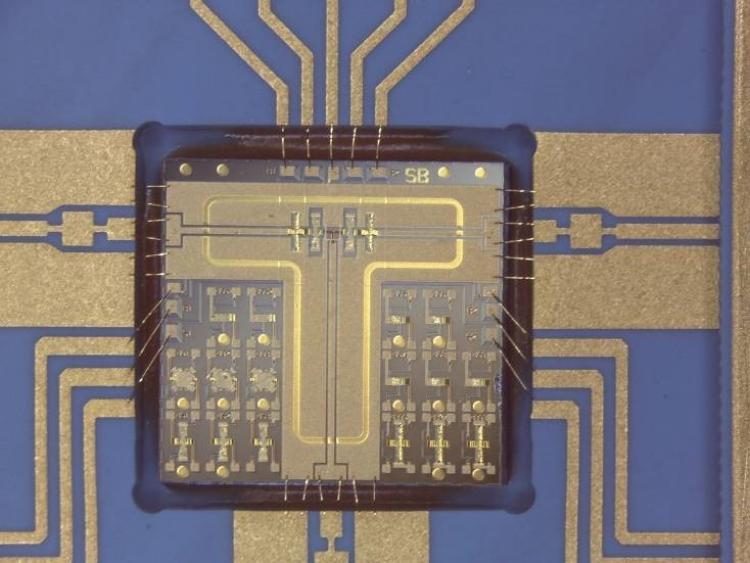
Within the MEMS/MOEMS research activities at IMM, high Technology Readiness Level (TRL) prototypes and demonstrators (up to TRL 5) have been produced.
Coordinator: Proietti Emanuela

The research aims to the development of MEMS using thin piezoelectric film deposited by sputtering process. In particular, the optimization of the deposition parameters, in order to obtain highly...
The research activities are addressed to the design and prototyping of:
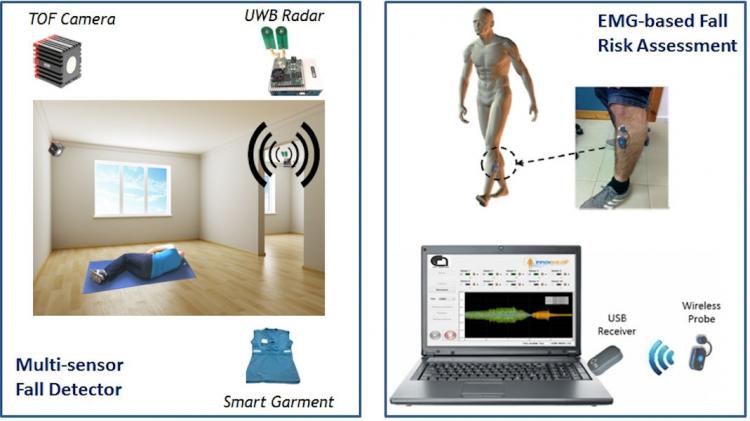
1. active (Time-of-Flight, Structured Light, RGB-D) and passive (RGB) vision systems for critical event prediction-...
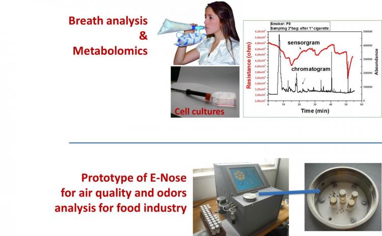
The development of future multifunctional chemical sensing devices requires multidisciplinary integration of different skills (physics, engineers, biologists, chemists, physicians) and...
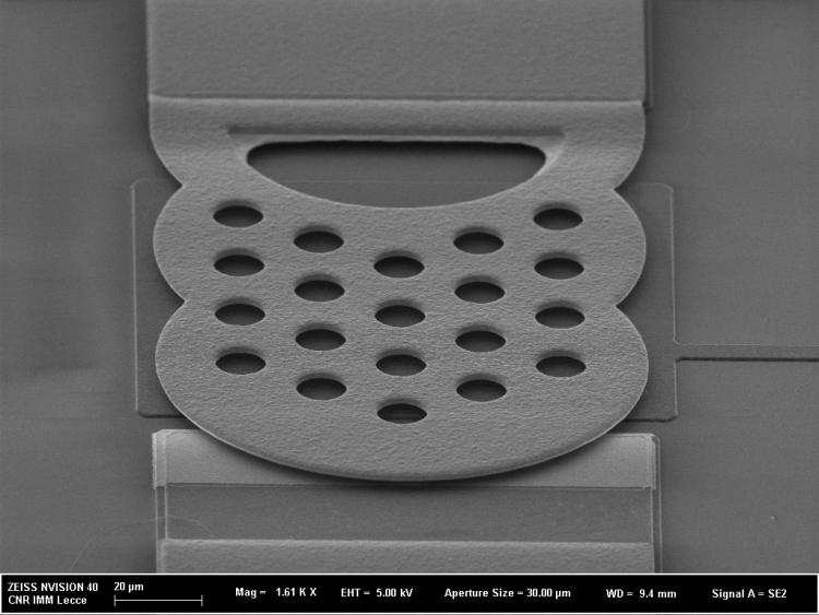
Development and study of new materials and technological processes for MEMS using surface or bulk micromachining, looking for full compatibility with...
The development of high frequency components and sub-systems has a driving market determined by many possible utilizations of the microwave and millimeter wave signal processing,...
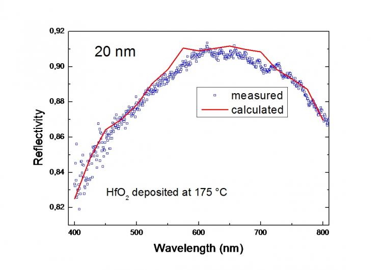
Due to the high conformality, excellent thickness control, availability of dense and pinhole free films of different materials at low deposition temperature and low cost, atomic layer deposition (...