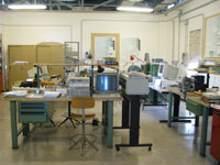
| Electrical Characterization Lab |
 |
|
- Suss PM5HF Analytical Probe System for DC and HF electrical measurements of samples up to 6 inches
- A second probe station for flexible substrates devices measurements
- A variable Temperature Micro-Probe System by MMR Technologies for electrical measurements of devices in vacuum in a temperature range of 80-580K
- Semicondutor Parameter Analyzer HP4145B for Dc electrical characteristics
- UV PERKIN ELMER Lambda35 Spectrometer
- FTIR PERKIN ELMER Spectrum 1000
- Keithley 236 Source measure unit
|
| |
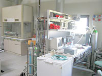
| Material Electrical Characterization Lab |
 |
|
- Digital Voltage Source Keithley k230
- Digital Current Source
- Quasi-static CV meter
- CV meter
- MKS Mass Flow Controller
- Keithley 6517A Electrometer
- Keithley 2001 Multimeter
- Hewlet Packard Multimeter
- Hewlet Packard Digital Oscilloscope
- Keithley 199 DMM Scanner
- Hewlet Packard Dynamic Signal Analyzer
- EG&G Lock in Amplifier
- Stanford Research Low Noise Amplifier
- Stanford Research Synthetized Function Generator
- Spectra Physics Laser
- MEMMERT Vertical Furnace
- Memmert Oven
- Vacuum Bell for electrical sensors characterization avoiding interfering gases
|
| |
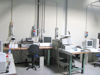
| Optoelectronic Lab |
 |
|
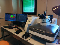
- Optical microscope (50x - 500x) with long working distance objective, digital photo and video cameras; the microscopes operates in transmission, reflection, polarized light, bright and dark and interference field (Nomarski technique) and conoscopy (Bertrand lens)
- Calibrated graded retardation plates (Berek) for measurements of optical retardation (Leica)
- Optical bench
- Hot stage (up to 250 °C) for microscope and bench use
- Fiber optics spectrophotometer for UV-VIS light, soon to be expanded to IR (<900 nm), for microscope and bench use
- Computer controlled precision translation and rotating stage setup
- Manually controlled translation and rotation stage system
- Solid state and He-Ne lasers
- Incoherent visible and UV light sources
- 500 Mhz, 4 channel, long memory digital sampling oscilloscope (LeCroy Waverunner 6050)
|
| |
| Millimetre and Microwave Design and Test Lab |
 |
|
- Autodesk AutoCAD for mask design
- Agilent ADS and AWR - Microwave Office for circuit simulations
- Comsol Multiphysics for electro-mechanics and electromagnetic simulations
- FORTRAN, MATHCAD and MATLAB for general purpose computations and graphics
- Agilent VEE for instrumentations remote control
- Ferromagnetic Resonance (FMR) waveguide equipment (magnetic materials line-width measurements at 9.25 GHz in a TE102 cavity)
- HP Spectrum Analyzer up to 22 GHz , for spectral measurements (phase noise, non-linear effects, …)
- HP8510C Vector Network Analyzer for S-parameter measurement up to 18 GHz
|
| |
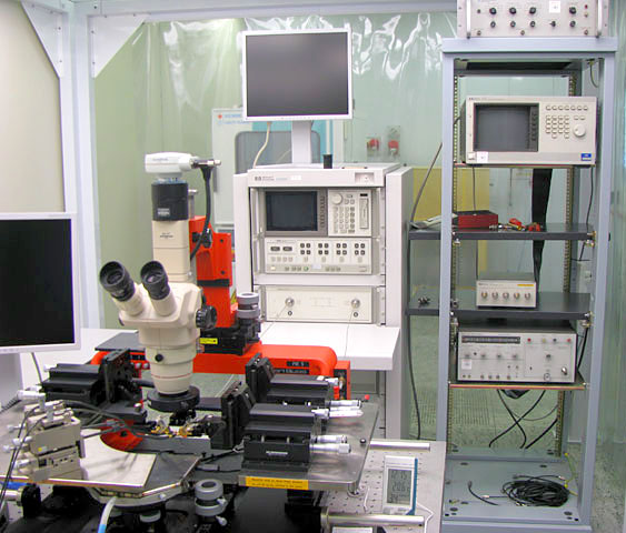
| On wafer Millimeter and Microwave Test Lab |
 |
|
On wafer Millimeter and Microwave Test Lab is dedicated to RF parameter measurement on environment condition sensitive devices. For this reason the entire lab is located in a special bay inside the clean-room facility.
- Probe Station for on wafer measurements up to 50 GHz A Karl Süss MP5 Probe Station equipped with Picoprobe / Karl Süss G-S-G high frequency probes and DC probes for testing coplanar structures up to 50 GHz is connected to a HP8510C Vector Network Analyzer, operation range frequency is from 45 MHz up to 50 GHz. Wafers from 1" up to to 4" can be mounted on a vacuum porous chuk. A nitrogen flux system is also available for lower the residual humidity down to 30% ca. in the test area. For the best tips and contacts positioning the probe station Olympus microscope is equipped with a high resolution video camera and a computer link-up allows a quick measurements elaborations
- HP8510C Vector Network Analyzer Analyzer for S-parameter measurement up to 50 GHz Microwave and millimetre wave characterizations of active and passive devices from 45 MHz to 50 GHz. The instrument can be remotely controlled via GPIB interface for automated measurement
- HP oscilloscope Digital oscilloscope for microwave and optical devices characterization up to 20 GHz
- Anechoic Chamber for millimetre wave antenna measurements (33-50 GHz). Covered inside by absorbing material to avoid EMI problems
- BIEMME T250 Thermostatic Chamber with a link to the Vector analyzer to perform S parameter measurements versus temperature from -40 C to 170 C. It can be used for the temperature response and aging of packaged devices
|
| |
| Millimetre and Microwave Materials and Process Lab |
 |
|
- Two vertical furnaces for LPE of magnetic films, temperature controlled and with automatic dipping and movements of the substrates
- Horizontal furnace for materials thermal annealing
- Logitech machine for materials lapping and optical polishing
- Kulicke & Soffa precision dicing machine (mechanical movement precision close to 1 µm) with 4" porous chuk, for allumina, silicon and garnet films cutting
|
| |
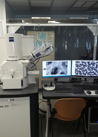
Scanning Electron Microscopy
Contact person annalisa.convertino@cnr.it |
 |
|
SEM, Zeiss Sigma 300
Zeiss Sigma 300 Field Emission SEM equipped with secondary and backscattered electron detectors, in-lens electron detector, and Bruker energy dispersive X-ray spectroscopy (EDS) system with dual silicon drift detectors.
Key Features
- Resolution:
- 1.2 nm @ 15 kV
- 1.6 nm @ 1 kV
- Accelerating Voltage: 0.02 kV – 30 kV
- Probe Current: 3 pA – 20 nA; 40 nA – 100 nA @ high current
|
| |
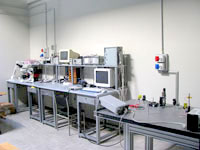
Vibrational Spectroscopy Lab - ViSLAB
Contact person valentina.mussi@cnr.it |
 |
|
-
Raman Imaging Microscope, DXR2xi Thermo Scientific
The microscope is used both for physico-chemical characterization of materials and devices, and for thermography applications, even in operating conditions. The instrument is equipped with two excitation lasers at 532 nm and 780 nm and two gratings with 5 cm-1 spectral resolution (FULL Range, 50-4000 cm-1 ) and 1 cm-1 spectral resolution (HIGH Resolution, 50-1800 cm-1 ). 10X, 50X, 50X long focal distance, 60X immersion objectives. Spatial resolution about 1 µm. Equipped with a thermal stage (THMS600 HEATING STAGE Linkam) to control and manage the sample temperature up to 600°C (also for liquid samples) with heating speed up to 150°C/min and temperature stability < 0.1°C.
-
Fourier Transform Infrared Spectroscope, Thermo Scientific Nicolet Summit FTIR
Equipped to work both in transmission and attenuated total reflection (ATR) configuration, for analysis on non-transparent samples in the IR, multilayers and powder samples.
|
| |
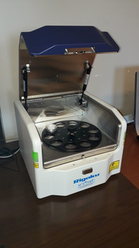
X-Ray Laboratory
Contact person raffaella.calarco@cnr.it |
 |
|
-
XRD Diffraction
The diffractometer is used for materials analysis, in particular in nanomaterials, microelectronics, and condensed matter scientific fields. Depending on the sample properties, particular parameters can be determined by X-ray analysis:
- Thickness, composition, mismatch, relaxation, and defects of epitaxial layers
- Thickness, roughness, and density of crystalline or amorphous layers
- Orientation identification and quantification of crystalline or textured layers
- In addition, the reaction of the parameters to temperature from 30° to 1100°C can be investigated
-
X-Ray fluorescence
Energy dispersive X-ray fluorescence (EDXRF) is used for the qualitative and quantitative determination of atomic elements in a wide variety of sample types. Diverse matrices, from homogeneous liquids of any viscosity to solids, thin films, alloys, powders and pastes, can be investigated. It provides rapid, non-destructive, multi-element analyses for elements from sodium (11Na) through uranium (92U).
|