
Electronic circuits fabricated by using large area compatible processes frequently employs materials with characteristics deeply different from those of the well-known materials used in crystalline silicon applications. The resulting devices have electrical characteristics that are often substantially different from their crystalline silicon counterpart, due to the different device physics associated to the specific materials and processes used. A successful circuit design requires a precise modelling of the device characteristics in all regimes of operation in addition to the availability of compact models that can be efficiently used in circuit simulation software environments. Hence, in addition to scientific motivations, there are also strong technological and industrial reasons in order to understand the phenomena that cause the device characteristics to behave differently from those of crystalline silicon devices and develop compact models that mimic that behaviors.
In IMM Rome Unit there is an ongoing research activity focused on the theoretical modelling of large area electronic devices that trace back to the early 90’s, with thorough investigation on the physics of amorphous and polycrystalline silicon thin film transistors (TFT). Currently, the theoretical research activity is mainly focused on the physics and modelling of organic thin transistors obtained by printing techniques, that are among the technologies candidate for ubiquitous electronics.
Some of the topics that are actively investigated are:
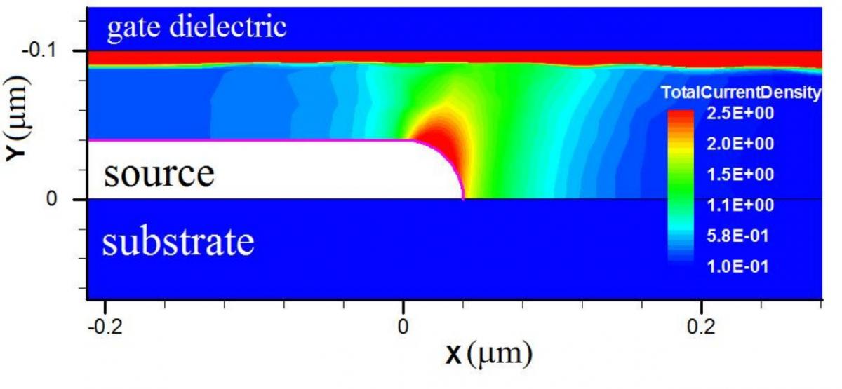
- Physics and modeling of contact effects. Metal/organic semiconductor junctions behaves much more like Schottky junctions than ohmic junctions, thus severely limiting the current in short channel devices. The characterization, simulation and modelling of the physics of charge injection at metal/organic semiconductor junctions and their impact on the static and dynamic behavior is of crucial importance when the scaling of the electrical characteristic with the device dimension is concerned.
- presence and energetic distribution of trapping states and charge transport mechanisms in the device active layer, that strongly impact on the maximum attainable field effect mobility and on the subthreshold characteristics.
- self-heating effects and device electrical stability upon prolonged bias stress in specific operating regimes and environmental conditions.
- Modelling of the small signal and large signal dynamic operation of organic TFT driven in non-quasi-static (NQS) regime. Due to the relatively small carrier mobilities of organic materials, is expected that organic devices enter in NQS regime at frequencies of the order of tens of kilohertz, thus making of fundamental importance the correct reproduction of the dynamic behavior even at such low frequencies.
|
|
The software tools used in this activity are:
- Synopsys® Technology CAD, a package for semiconductor based device and process simulation at microscopic/nanoscopic scale, using semiclassical approaches
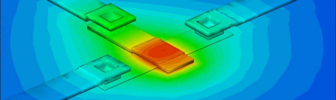
- COMSOL® Multiphysics for finite element modelling
- CADENCE® Virtuoso, a package for circuit simulation and layout automatic generation and verification