
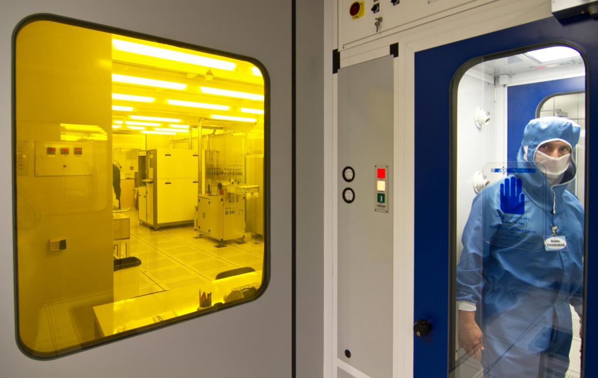
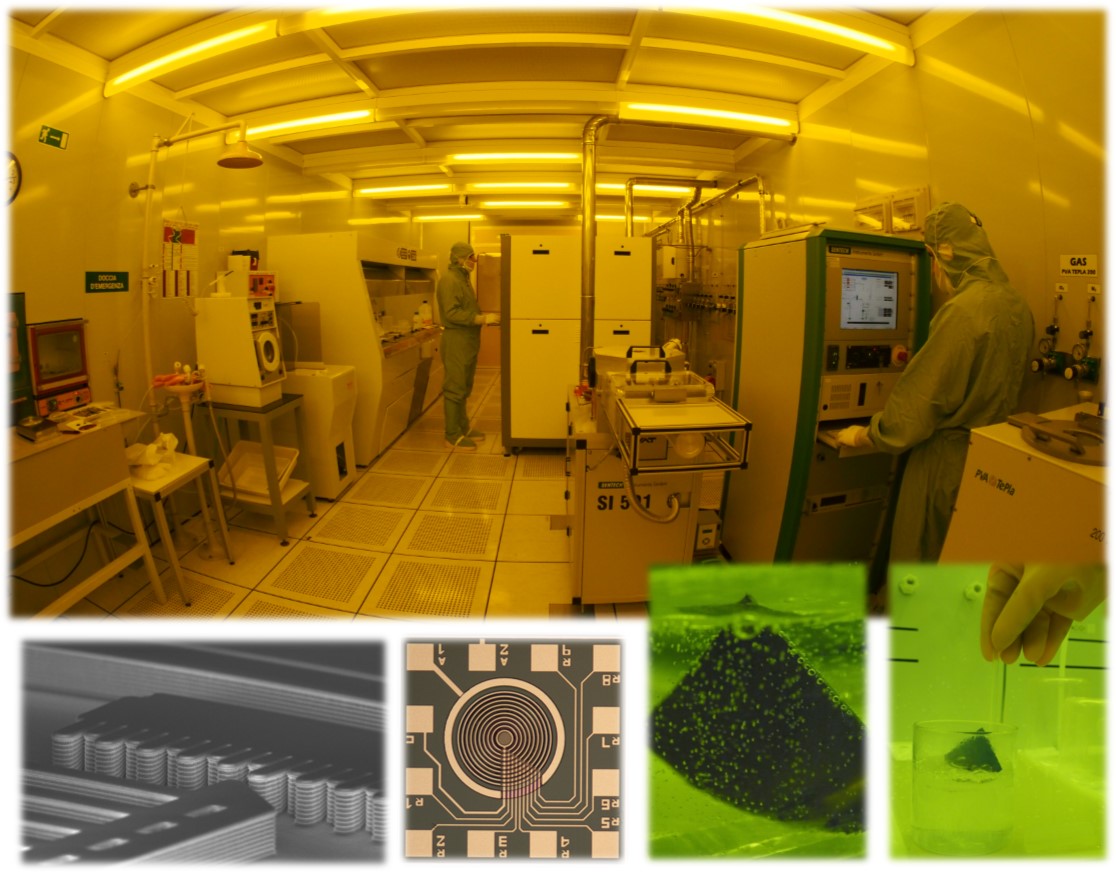
Peculiar of IMM Bologna facilities is the availability of a 500 m2 clean-room, with 100 (ISO 5) and 100000 (ISO 8) class laboratories, fully equipped with the main technological instrumentations for performing research in the fields of micro-nano electronics and micro-systems.
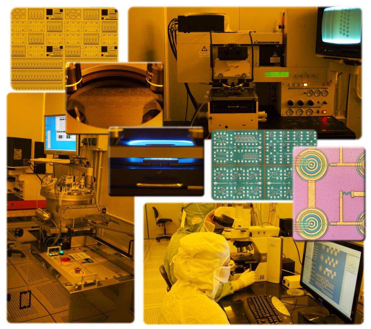
A distinctive characteristic of IMM Bologna is represented by the capability to face studies on materials and processes as well as to develop and manufacture high TRL prototype devices (integrated circuits, solar cells, sensors, actuators, microfluidic chips …) with the possibility of small-scale productions.
Starting substrate materials are typically 4” wafers of silicon, silicon carbide, lithium niobate and glass.
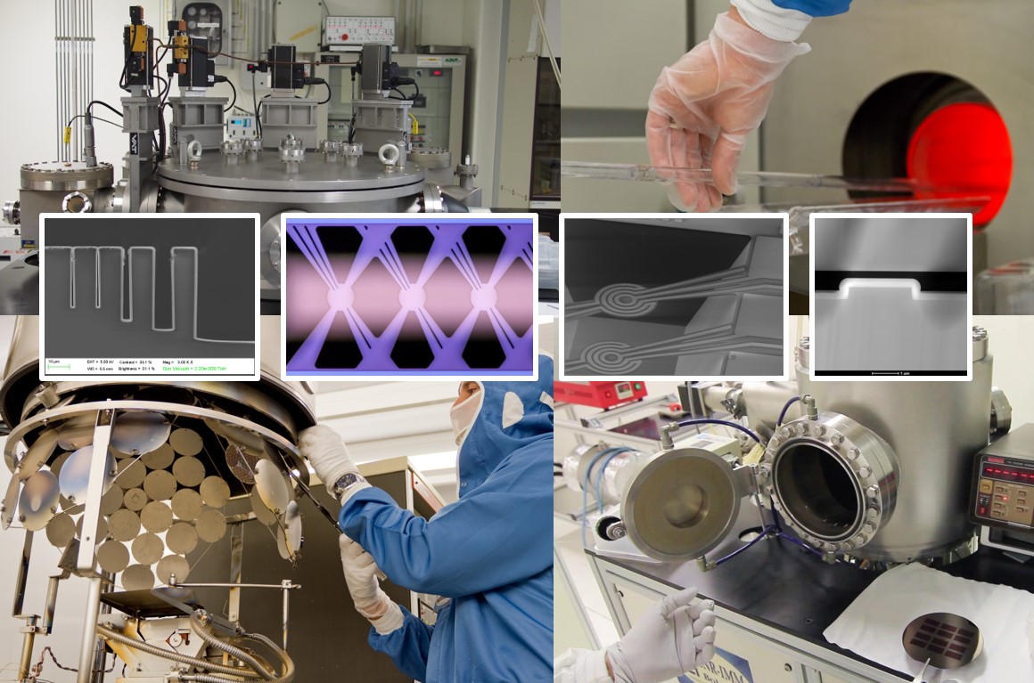
The Clean Room is organized in 9 different technological areas, each dedicated to a specific processing applications.
|
|
IMM Bologna Clean Room infrastructure is inside the Italian network of research infrastructures in the field of nanofabrication (It-Fab) |
CLEAN ROOM BROCHURE (CLEAN ROOM BROCHURE.pdf)
| OPTICAL PHOTOLITHOGRAPHY | |
|
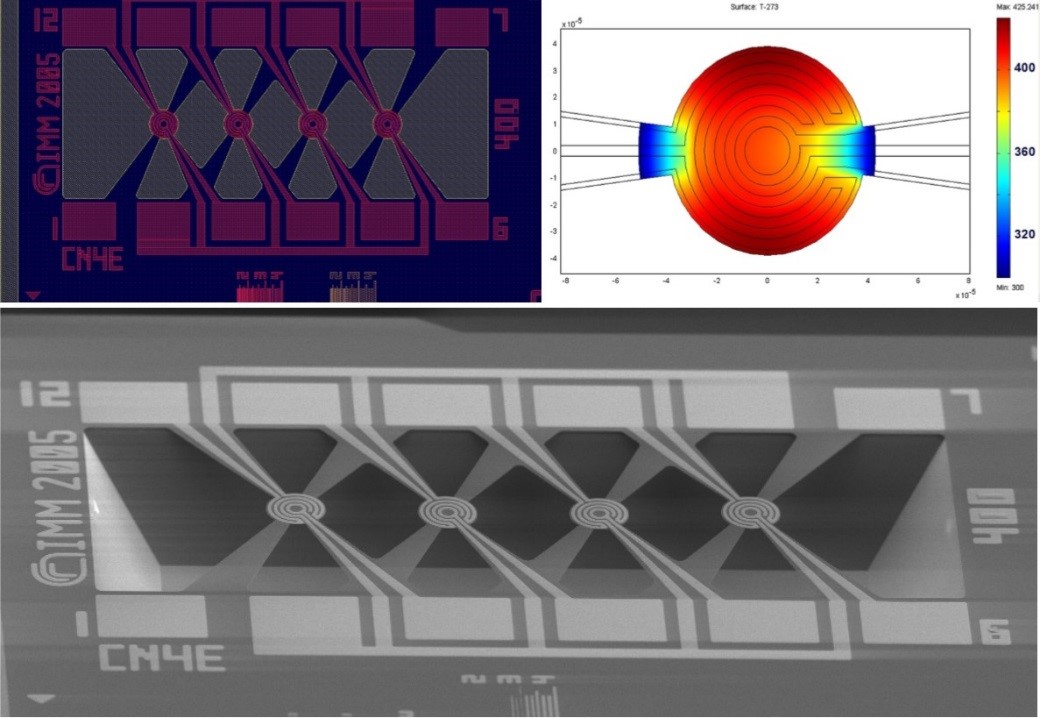
The laboratory comprises all the facilities to define micropatterns on planar substrates by means of optical lithographywith a resolution down to 700 nm. Equipment for alignment and bonding between two or more wafers for MEMS device fabrication are also available.
CONTACT PERSON: FILIPPO BONAFE' |
|
| NANOLITHOGRAPHY AND NANOPROCESSING | |
|
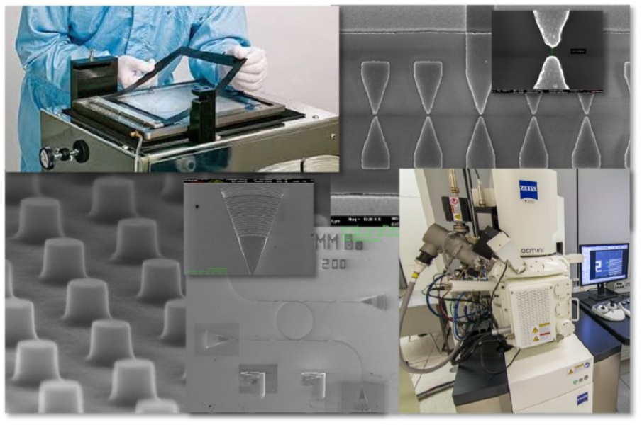
Individually or in combination with e-beam lithography, the SCILL NIL system can be used for large-area device nanofabrication. Nano Imprint Lithography (NIL) is an emerging lithographic technology that promises high throughput patterning of nanostructures. With NIL it’s possible to achieve sub-50nm resolution features over large areas. NIL can significantly simplify the production of nanostructures using a wide variety of materials. NIL intrinsically has better dimensional control that can be achieved using conventional UV lithography |
|
| WET AND DRY ETCHING | |
|
This laboratory is dedicated to isotropic and anisotropic etching (both along crystal planes and with high aspect ratio) of thin films and bulk materials by wet and dry processes. Here are located also the facilities for substrate and photolithographic mask surface cleaning.
CONTACT PERSON: FABRIZIO TAMARRI |
|
| GROWTH, DEPOSITION AND THERMAL PROCESSES | |
|
The laboratory includes facilities dedicated to deposition and growth on wafer substrates of several materials such as dielectric (TEOS, LTO, Si3N4, gate oxides) and conductive (a-Si and Polysilicon, metals, CNT, Graphene) layers. Moreover, it is possible to perform several types of thermal treatments including annealing (silicon/polysilicon up to 1100 °C, SiC up tp 1900 °C, and metals in FG) and diffusion doping. |
|
| MICROSYSTEM PROCESSES | |
|
The Microsystems Laboratory is a semiconductor processing facility specializing in the fabrication of various types of chemical, physical sensors and multifunctional microsystems. The facility consists of more than 50 m2 of Class 10 clean room space. Process capabilities Deep plasma etching, wet anisistropic silicon etching, deep glass wet etching and wafer bonder. The microsystem laboratory works in synergy with all the other laboratories |
|
| ION IMPLANTATION | |
|
The laboratory is dedicated to the doping of semiconductor wafers by ion implantation at high and low energy. The same equipment are also used for performing surface treatments and material analyses with selected ion beams.
CONTACT PERSON: MICHELE BELLETTATO |
|
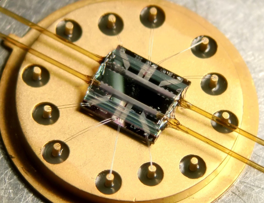
| PACKAGING | |
|
The packaging laboratory comprises all the equipment necessary to separate a substrate wafer in dies and electrically and fluidically connect the die into a package. |
|
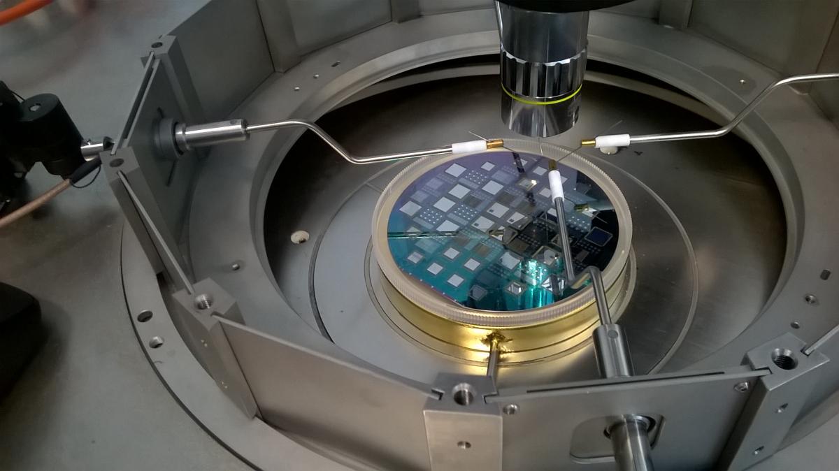
| METROLOGY, CONTROL AND ELECTRICAL CHARACTERIZATION | |
|
The laboratory is dedicated to perform the measurements necessary for on-line verification of process steps and to evaluate the electrical performances on test structures and devices at wafer level. Both manual and automatic systems are available. |
|
| SIMULATION AND DESIGN | |
|
This facility comprises the design and simulation tools necessary to support the fabrication of microelectronic devices and MEMS. Available software packages include all the steps from the modelling of the devices to the design of the fabrication masks and the definition of the technological process flow. |
|