
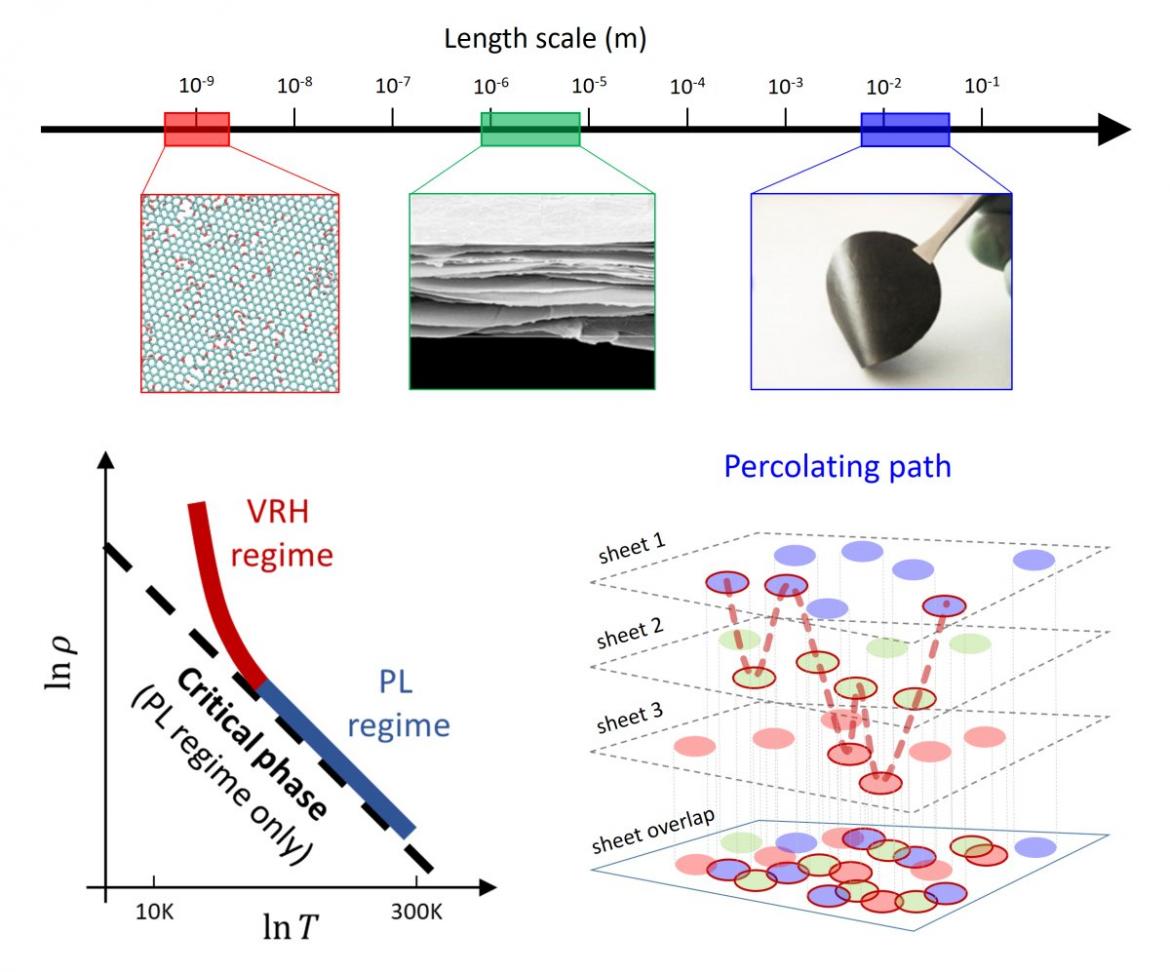
Large area van der Waals (vdW) thin films are assembled materials consisting of a network of randomly stacked nanosheets. The multi-scale structure and the two-dimensional nature of the building block mean that interfaces naturally play a crucial role in the charge transport of such thin films. While single or few stacked nanosheets (i.e. vdW heterostructures) have been the subject of intensive works, little is known about how charges travel through multilayered, more disordered networks. Here we report a comprehensive study of a prototypical system given by networks of randomly stacked reduced graphene oxide 2D nanosheets, whose chemical and geometrical properties can be controlled independently, permitting to explore percolated networks ranging from a single nanosheet to some billions with room temperature resistivity spanning from 10-5 to 10-1 Ω×m. We systematically observe a clear transition between two different regimes at a critical temperature T*: Efros-Shklovskii variable range hopping (ES-VRH) below T* and power law (PL) behavior above. Firstly, we demonstrate that the two regimes are strongly correlated with each other, both depending on the charge localization length ξ, calculated by ES-VRH model, which corresponds to the characteristic size of overlapping sp2 domains belonging to different nanosheets. Thus, we propose a microscopic model describing the charge transport as a geometrical phase transition, given by the metal-insulator transition associated with the percolation of quasi-1D nanofillers with length ξ, showing that the charge transport behavior of the networks is valid for all geometries and defects of the nanosheets, ultimately suggesting a generalized description on vdW and disordered thin films.
DOI: 10.1021/acsnano.0c07771
Contact: Dr. Andrea Liscio (andrea.liscio@cnr.it)