
Characterization at Agrate Brianza Unit
Characterization at Agrate Brianza is focused on the study of materials and devices for the microelectronic research and industry with a portfolio of advanced techniques. The challenge is to quantitatively determine chemical, structural, optical, electrical and magnetic properties of very thin films, in the scale of few nm thickness and down to the single atomic layer, and their surfaces or interfaces. Actions are undertaken with state-of-the-art instrumentation with advanced facilities, in many cases specifically designed or adapted in our laboratory. Expertise is related to the use of Scanning probe techniques, X-ray diffraction, reflectivity and fluorescence, Time of Flight Secondary Ion Mass Spectrometry, X-ray Photoelectron Spectroscopy, Raman(visible, UV) (FT)IR-UV-Vis Spectroscopies, Ellipsometry, Mössbauer spectroscopy, Electron Paramagnetic Resonance, Magneto-transport and Electrical characterization.
Characterization methods are mainly targeting two dimensional materials, materials and devices for non-volatile memories and neuromorphic applications, MIM capacitors, MOS structures and transistors, quasi-static and dynamic evaluation of single and multiple quantum dots in presence of microwaves and magnetic field. Agrate Unit has strong interactions with academic and industrial research centers devoted to microelectronics worldwide.
Research is facilitated by the presence of multiple instrumentation at the same site (inside STMicroelectronics with 24 hours/day regulated access) and by the habit of the experienced researchers to work in multidisciplinary and international teams. Scientific collaboration is envisaged for all the characterization experiments. Commercial collaborations are possible, after discussion and approval. Preliminary measurements, often free of charge, are encouraged.
Please don’t hesitate to contact Lamperti Alessio or the person in charge of the specific instrument.
Characterizations are categorized in the following general fields:
Morphological, Structural and Chemical characterizations
Electrical, Electro-chemical and Magneto-electrical characterizations
Optical characterizations

Electron microscopy and Scanning probes
Scanning electron microscopy (SEM): Sabina Spiga
Scanning probes: Graziella Tallarida, Stefano Brivio
Chemical methods
Time of Flight Secondary Ion Mass Spectroscopy (ToF SIMS): Michele Perego, Alessio Lamperti
X-ray photoelectron Spectroscopy (XPS): Alessio Lamperti, Michele Perego
X-ray methods
X-ray Diffraction, Reflectivity, Fluorescence (XRD, XRR, XRF): Claudia Wiemer, Alessio Lamperti
Hyperfine structure methods
57Fe and 119Sn Conversion electron Mössbauer spectroscopy (CEMS): Roberto Mantovan
On-line Mössbauer spectroscopy @ ISOLDE-CERN: Roberto Mantovan
Electron paramagnetic Resonance: Matteo Belli, Marco Fanciulli
Contact Persons: Sabina Spiga
Instrument name: ZEISS Supra40 field emission scanning electron microscopy
Technical characteristics:
- High performance featuring the GEMINI® column.
- Schottky field emitter.
- Resolution
- 1.0 nm at 20 kV at WD = 2 mm
- 1.3 nm at 15 kV at WD = 2 mm
- 1.5 nm at 10 kV at WD = 2 mm
- 2.1 nm at 1 kV at WD = 2 mm
- 5.0 nm at 200 V at WD = 2 mm
- Acceleration Voltage Range: 0.1 - 30 kV
- Probe Current Range: 4 pA - 20 nA,
- Chamber Detectors: Everhart-Thornley SE-detector with optically coupled photomultiplier. CCD-camera with IR-illumination.
- In-lens Detector Type: High efficiency annular scintillator detector mounted in GEMINI column with optically coupled photomultiplier.
Materials/devices to be analysed: semiconductors, devices, nanostructures (nanowires, nanodots, etc)
Samples: chamber dimension: 330 mm inner diameter and 270 mm height for large samples. Current sample holder for small samples (1x1 to 4x4 cm2), able to take images of wafers up to 4-6” albeit with limited stage motion. Sample holder for both plan and cross-section view.
back to Morphological, Structural and Chemical Characterizations
Contact Persons: Graziella Tallarida, Stefano Brivio
Instrument name
- Bruker - In air: AFM, STM, MFM, EFM, SCFM, KPFM, TUNA
- Omicron – In UHV: and at variable temperature (25-1200 K): AFM, STM, KPFM, BEEM
Technical characteristics
- In air: Spatial resolution on the surface plane is few nm. Maximum scan range 100x100 micron2.
- In UHV: Atomic resolution achievable in all the temperature range
Materials/devices to be analysed
- Main expertise in investigating hard surfaces (semiconductors, metals and insulators, 2D-materials).
- Main expertise in the in-situ investigation of the atomic arrangement of flat and prepared surfaces by STM and STS.
Samples
- it is possible to measure entire wafers up to 6”, as well as small pieces of any size. A sample navigator system allows to precisely locate the measurement area
- only small samples (12-14 mm side) can be measured.
Key features/expertise
- Commercial equipment. It is equipped for performing conductive-AFM with high sensitivity and with double lock-in for Kelvin Probe Force Microscopy. Solid expertise has been developed in the investigation of the local electrical properties of materials for RERAM by conductive-AFM and KPFM
- The scanning probe tool is commercial (Omicron) and is mounted in the UHV system that includes MBE growth facility and XPS. It has been extensively used for the characterization of silicene.
Relevant publications
- Jacopo Frascaroli et al., ACS Nano 9 , 2518–2529 (2015)
S Brivio, et al., Nanotechnology, 25 385705 (2014) - D. Chiappe, et al., Advanced Materials 24, 5088 (2012)
D. Chiappe, et. al., Adv. Mater., 26: 2096–2101 (2014)
back to Morphological, Structural and Chemical Characterizations
Contact Persons: Claudia Wiemer, Alessio Lamperti
Instrument name
- HRXRD IS2000 for XRD and XRR.
- HRXRD IS3000 for XRF, TXRF and XRR
Technical characteristics
- Goebel mirror monochromator, 4 circle goiniometer, scintillator and position sensitive detector, equipped with Anton Paar sample holder for measurements vs temperature (RT-1200°C) in N2 or air. All the geometries for diffraction and x-ray scattering are in principle possible.
- Instrument equipped with a solid state detector and a scintillator, for the simultaneous detection of x-ray reflectivity and x-ray fluorescence.
Materials/devices to be analysed
- Thin inorganic films from 2 nm to 1 mm (less experience for the study of organic materials)
- Any surface, particular of interest for the detection of contaminant and for the determination of stoichiometric ratio in thin films. Reveals elements with Z>Al.
Samples
- Size ranging from 1 mm2 to 8 inches, possibility to scan x and y with 1/100 mm step. Sample maximum 2x2 cm2 for in situ XRD vs T.
- Size ranging from 1cm2 to 2 inches.
Key features/expertise
- Instrument developed within the framework of the European Project (ESQUI: 2001-20014, RTD project n. GRD1-1999-11097) with the specific purpose of advancing x-ray diffraction and x-ray reflectivity characterization for thin films for the microelectronic industry. The combination of a position sensitive and a scintillator detector allows the precise measurement of sample thickness by x-ray reflectivity and x-ray diffraction analysis with enhanced signal to noise ratio, reducing the acquisition time and enhancing sensitivity to ultra thin films. The Instrument was then commercialized by Italstructures (Riva del Garda). The use of this instrument and the refinement of the data is of particular relevance for the microelectronic industry, in particular since the era of high-k materials, it reveals the signature of crystallization in thicknesses that were only accessible by TEM.
- The instrument was especially designed to determine the chemical composition of thin films of ternary chalcogenide alloys for phase change memories applications in the framework of the European project Chemaph (EU IST Project # 027561, 2006-2008). The combined detection of x-ray fluorescence and specular reflectivity allows on one hand the precise alignment of the sample to enhance the total external reflection, and therefore the sensitivity, for very thin films, on the other to perform, in principle, depth profiling of the chemical composition. An upgraded version of Maud software, developed in 2015, allowed for this analysis.
Relevant publications
- Wiemer C. et al., Thin Sol. Films. 450/1, 134-137 (2004)
Colombi P. et al, J. Appl. Cryst. 41, 143–152 (2008)
Lamperti A. et al., Journal of The Electrochemical Society, 158 (10) G221-G226 (2011) - O. Salicio et al, Journal of Applied Physics 105 , 033520 1-6 (2009)
Massimo Longo et al., Nano Letters 12, 1509-1515 (2012)
back to Morphological, Structural and Chemical Characterizations
Contact Persons: Michele Perego, Alessio Lamperti
Instrument name: TOF SIMS ION-TOF IV
Technical characteristics: Dual beam analysis. Ga primary ion (analysis 50x50 um2). Cs and O2 sputtering ions Time of flight analyzer: mass resolution > 10000 Detection limit ppm-1% Depth resolution < 1 nm Lateral resolution > 50 nm
Materials /devices to be analysed: Thin dielectrics (oxide of transition metals and rare earths); Nanoclusters (P, SiO) in Si or SiO2; profile doping and element diffusion.
Samples: Thin films and multilayers at the nanoscale (typically max 100-200 nm depth scale); sample dimension min. 5 mm x 5 mm, max 15 mm x 30 mm, typical 10 mm x 10 mm) Sample holder: max 12-14 samples 10 mm x 10 mm. 8” wafer possible on special holder upon request.
Key features/expertise: Profile doping Contamination microanalysis CMOS compatibility Nanostructures and nanoclusters 2D materials Structure evolution upon different treatment (growth conditions, annealing, reactant, chemical environment) Interest also for biological or bio-inspired systems.
Relevant publications:
Alessandro Molle, et al., Advanced Materials Interfaces (2016)
R. Lo Conte, et al., Physical Review B 91, 014433 1-9 (2015)
Michele Perego et al., Nanoscale 7, 14469–14475 (2015)
M. Mastromatteo et al., Journal of Materials Chemistry C, (2016)
back to Morphological, Structural and Chemical Characterizations
Contact Persons: Alessio Lamperti, Michele Perego
Instrument name: XPS ESCA PHI 5600
Technical characteristics: Al monochromatic source 7mm & 2mm filaments; max 8 sample holders carrousel; angle resolved possible; Energy resolution 0.1 eV
Materials /devices to be analysed: Thin dielectrics; Si nanoclusters; 2D materials.
Samples: Thin films; depth resolution down to few nm unless ion sputtering analysis; 15 mm X 15 mm max dimensions. Typical 2 pieces 10 mm X 10 mm in 1 sample holder.
Key features/expertise: band alignment; study on confined structures (nano-clusters, nanostructures, 2D materials)
Relevant publications:
S. Vangelista, et al., Nanotechnology 27 (2016) 175703
Michele Perego, et al., Nanoscale 7, 14469–14475 (2015)
back to Morphological, Structural and Chemical Characterizations
Contact Persons: Matteo Belli, Marco Fanciulli
Instrument name: Bruker Elexsys E580 Electron Paramagnetic Resonance Spectrometer
Technical characteristics: Continuous wave and pulsed EPR in X-band and continuous wave EPR in Q-band in the temperature range from 4.2 K to 300 K
Materials /devices to be analysed: Paramagnetic samples or samples containing paramagnetic centers.
Samples: X-band: ~1.2 cm x 3.5 mm; Q-band: 2-6 mm x 1.5-2 mm
X-band sample access: 4 mm, Q-band sample access: 3 mm).
Key features/expertise: The instrument is generally employed for the investigation of donors or defects in silicon and silicon nanostructures.
Relevant publications:
M. Fanciulli et al., ECS Journal of Solid State Science and Technology 5, P3138 (2016)
M. Belli et al., Phys. Rev. B 89, 115207 (2014)
M. Belli et al., Phys. Rev. B 83, 235204 (2011)
M. Fanciulli et al., Phys. Rev. B 74, 134102 (2006)
back to Morphological, Structural and Chemical Characterizations
On-line Mössbauer Spectroscopy @ ISOLDE-CERN
Contact Person: Roberto Mantovan
Instrument name: Mössbauer Spectroscopy (MS): conversion electron-MS (CEMS) and emission-MS (eMS)
Technical characteristics: Hyperfine interactions-based methods to conduct atomic-scale structural, chemical, magnetic studies in Fe, Sn-containing materials (lattice site, charge state, local symmetry/magnetism). Element-selective and non-destructive techniques.
Materials /devices to be analysed: CEMS: Sn, Fe -based thin films (Fe, Fe3O4, Fe3Si, Fe/oxides interfaces, Sn and Sn oxides,) eMS: Si, Ge, ZnO, TiO2, Al2O3, SnO2, dilute magnetic semiconductors/oxides, MnSi, MnGa, NiMnSn(In), nitrides, chalcogenides,… (in principle no limits), following their implantation with radioactive 57Mn/57Co/119In ions.
Samples: CEMS: 1 x 1 cm2 thin films containing Fe and Sn. Typically 57Fe and 119Sn enriched samples are necessary, but in some systems (es: Fe3O4) also only with natural Fe if thickness ≥30 nm. eMS: 1 x 1 cm2 thin films (minimum thickness to valuate depending of implanted ion projected range in specific materials) and single crystals (max thickness: few mm).
Key features/expertise: CEMS: a dedicated parallel-plate avalanche counter (PPAC) operating from 295 K down to 100 K has been home-built in Agrate, and it is one of the few options for low temperature CEMS worldwide. When compared to standard lab. MS techniques, eMS is performed at extreme dopant dilution down to 10-4 at.%, being unique in providing atomic-scale probes to investigate materials in a regime of extreme dilution. Different custom-built sample mounting stages are available allowing to implant/measure in the 90-700 K temperature range, at variable angles, in 0.6T permanent magnetic field. Also quenching experiments are possible to get rid of implantation damage components. Researchers in Agrate B. have a long-standing experience in making use of the large-scale facility of ISOLDE at CERN to perform on line eMS in the framework of an international collaboration (http://e-ms.web.cern.ch/)
Relevant publications:
A.Zenkevich et al., Appl. Phys. Lett. 99, 182905 (2011)
H.P. Gunnlaugsson et al., Appl. Phys. Lett. 97, 142501 (2010)
back to Morphological, Structural and Chemical Characterizations

Scanning probes methods
Kelvin Probe Force Microscopy (KPFM) Graziella Tallarida, Stefano Brivio
Conductive Atomic Force Microscopy (C-AFM) Graziella Tallarida, Stefano Brivio
Magnetic Force Microscopy (MFM) Graziella Tallarida, Stefano Brivio
Electrostatic Force Microscopy (EFM) Graziella Tallarida, Stefano Brivio
Electrical and electro-optical methods
Probe stations for AC/DC/pulsed measurements Sabina Spiga, Stefano Brivio
Internal Photoemission Spectroscopy (IPE) Gabriele Seguini
Magneto-electrical methods
Magneto-transport facility (Magnetoresistance) (4.2-300K, 1T, angular dependence) Roberto Mantovan
Quantum transport (Cryomagnet @ He temperature): Marco De Michielis, Matteo Belli, Marco Fanciulli
Hall effect measurement system Roberto Mantovan
Contact Person: Roberto Mantovan
Instrument name: Magnetotransport
Technical characteristics: Magnetotransport (5-300 K) up to 1.1 T at variable angles wit h respect to sample’s plane (0°-90°)
Materials/devices to be analysed: Hall: semiconductors, chalcogenides. MR: Ferromagnetic thin films (Fe3O4, Fe,..) and patterned structures (spin valves, Hall bars, magnetic
Samples: Two sample holder available: 1. Up to 1 x 1 cm2 area for simultaneous rho, I-V, Hall, MR measurements in the Van der Pauw geometry and custom 2-point configurations (I-V, R, MR). Up to 4 x 8 mm2 samples with patterned structures to be bonded on chip
Key features/expertise: Close cycle cryostat, 24h measurements possible; home-built system for rotating the samples in the applied magnetic field; home-built LabVIEW-based software with possibility to run temperature-dependent simultaneous rho, I-V, Hall, MR measurements overnight/over the weekend
Relevant publications:
R. Mantovan et al., J. Phys. D 43, 065002 (2010)
Roberto Fallica, et al., Applied Physics Letters 101, 102105 (2012)
back to Electrical, Electro-chemical and Magneto-electrical Characterizations
Contact Person: Marco De Michielis, Matteo Belli, Marco Fanciulli
Instrument name: Quantum transport measurements on semiconductor devices
Technical characteristics: 12T Superconducting Cryomagnet 270mK Cryostat Technical characteristics Cryogenics 3He cryostat with base temperature down to 300 mK. Magnetic field up to 12 T. Possibility to transmit electric signals and microwaves toward the sample through a top-loading probe. Sensing of small electric signals due to a low noise cryogenic amplifier located on the probe shaft. Probe tip provided with a rot or for sample spatial orientation.
Materials/devices to be analysed: Quantum transport measurements on semiconductor devices. Expertise in the quasi-static and dynamic electrical characterization of single and multiple quantum dots devices in presence of microwaves and magnetic field.
Samples: Typical measured devices are single and multiple quantum dot electrostatically and lithographically defined in the tens of nms size scale. Sample size compatible with a Dual In Line (DIL) socket.
Key features/expertise: The overall system is a commercial one with a custom probe that has been modified, during time, to host a low noise electronic amplifier. The system will be used in the H2020 ICT project (Grant Agreement n° 688539, MOS-QUITO). In this project, CMOS technology will be exploited to fabricate nanodevices to benchmark different architectures of quantum bits (qubits) based on spin states of confined electrons. The cryostat will provide the physical conditions (low temperature, EMR shielded environment, constant magnetic field) that, together with the probe performances (electrical interconnections with low parasitics) and with the low noise electronics, will let us perform initialization, manipulation and readout activities on one promising qubit architecture.
Relevant publications:
M. L. V. Tagliaferri, et al. ,IEEE Transaction on Instrumentation and Measurements 65, 1827-1835 (2016)
E. Prati et al. Nanotechnology 23 215204, (2012)
G. Mazzeo et al., Applied Physics Letters 100 (21) 213107, (2012)
back to Electrical, Electro-chemical and Magneto-electrical Characterizations
Contact Person: Sabina Spiga, Stefano Brivio
Instrument name: The electrical lab for the device testing is equipped with two 6” probe stations and related rack for DC and AC testing (setup1 and 2), and one cryogenic manipulator (setup3). The instruments can be adapted if necessary to different setups
Setup1: Agilent B1500A Semiconductor Device Parameter Analyzer with fours SMU and High Voltage Semiconductor Pulse Generator Unit( B1525A-FG); Agilent 81110 Agilent Pulse Pattern generator, 1 GHz Agilent MSO6104A oscilloscope; custom switch board for pulsed setup
Setup2: HP 4140B pA meter, Agilent E4980 precision LCR meter, PerkInElmer7265 DSP Lock-in Amplifier, Agilent oscilloscope 54622A, Keithley 6430 SubFemto Amp Source Meter
Setup3: TTP-4 probe station (4K-400 K); Lakeshore331 temperature controller, Stanford Lock-in SR830 DSP Lock-in Amplifier; Boonton72B Capacitance Meter, HP 4284A LCR meter, H P 4140B pA meter
Technical characteristics:
Current-voltage (IV) measurement capabilities of spot, sweep, and pulse measurement in the range of 0.1 fA - 1 A / 0.5 µV - 200 V
AC capacitance measurement in multi frequency from 100 Hz to 2 MHz
Advanced pulsed IV capability, up to 40 V high voltage pulse forcing fo r non-volatile memory evaluation
Materials/devices to be analysed: RRAM non volatile memory, MOS and MIM capacitors, transistors, test device on novel materials
Samples: Devices from 1x1 cm2 to 6” at room temperature, 2x2 cm2 for the TTP-4 probe station
Key features/expertise: Several type of measurements available. Dedicated software developed in-house with Labview, custom interface switching boards
- Versatile characterization of RRAM and memristive devices, switching dynamics, endurance, retention
- Capacitance- voltage and current-voltage of MOS and MIM devices, as a function of temperature, low current measurements
- Transistor characterization
Relevant publications:
S.Brivio et al., Appl. Phys. Lett. 107, 023504 (2015)
S. Spiga et al., J. Appl. Phys. 112, 014107 ( 2012)
back to Electrical, Electro-chemical and Magneto-electrical Characterizations

Raman
Visible and UV Micro Raman / Micro PL spectroscopy: Alessandro Molle, Alessio Lamperti
Micro-Raman / Micro PL spectroscopy
(multi wavelength, vis, UV, 2D maping, thermal & cryogenic stage)
Infrared, visible, UV
Fourier-Transformed Infrared Spectroscopy (FTIR) Alessio Lamperti, Alessandro Molle
Ultraviolet-Visible-near Infrared Spectrophotometry (UV-Vis-NIR) Alessio Lamperti
Spectroscopic Ellipsometry (SE): Elena Cianci
Contact Person: Alessandro Molle, Christian Martella
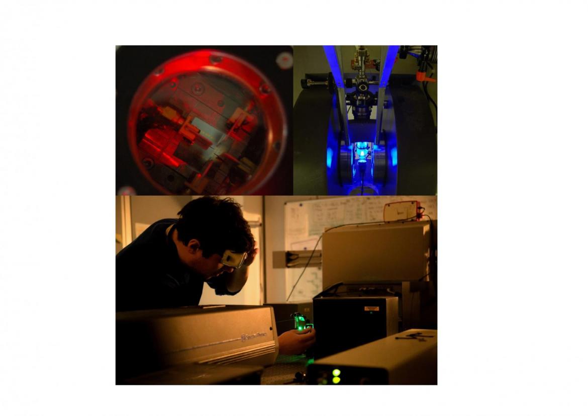
Instrument name: Renishaw InVia Multiwavelength micro-Raman spectroscopy
Technical characteristics: Excitation wavelength in the visible (488 nm, 514nm, 633 nm) and in the UV (364 nm), macroscopic map acquisition; Renishaw Invia Analyzer; Renishaw RM100 Analyzer
Materials/devices to be analysed: Silicon, 2D materials, silicene, transition metal dichalcogenides, phosp horene, Germanium, silicides
Samples: Bulk, thin films, 2D materials (sample or support size up to several cm2
Key features/expertise: MicroRaman spectroscopy is mainly developed in our unit to discern: -local stress induced in silicon structures -number of sheets and atomic ordering in 2D materials (silicene, germanene, MoS2). The activity has recently been shared with international partners in the framework of a European FET project: 2D-nanolattices (http://www.2dnanolattices.eu/) and CNR grant – Laboratori Congiunti con Univ. Texas at Austin, USA, and CARIPLO-Regione Lombardia grant "CrystEL"
Relevant publications:
F. Fabbri et al., Nat Comm. 7, 13044 (2016)
E. Cinquanta, et al., J. Phys. Chem. C 117, 16719 (2013)
back to Optical Characterizations
Contact Person: Alessio Lamperti
Instrument name: Bruker IFS66v/S
Technical characteristics: Spectral range: 100 - 4000 cm-1; spectral resolution <0.1 cm-1; signal-to-noise: peak-to-peak noise < 10-5 AU (1 minute, 4 cm-1 spectral resolution);
time resolved spectroscopy: more than 100 spectra/sec rapid Scan at 12 cm-1 spectral resolution, step scan temporal resolution of <10 nsec in the mid IR, slow Scan < 0.006 cm/sec optical velocity
Stage for reflectivity geometry at variable angle.
Materials/devices to be analysed: Thin film thickness analysis and anti-reflection coating analysis; analysis of novel nanocomposite materials.
Samples: Solid: minimum size 0.5 cm x 0.5 cm.
Key features/expertise: Optical response of dielectric thin films, dopants in Si.
back to Optical Characterizations
Contact Person: Alessio Lamperti
Instrument name: Instrument name Agilent Tecnologies Cary 5000
Technical characteristics: spectral range: UV, Vis, NIR 175÷3300 nm; bandwidth: UV-Vis 0.01-5 nm, NIR 0.04-20 nm; photometric range: 8 Abs; Source: UV Deuterium, VIS-NIR Tungsten, Reference and calibration Mercury; Source optics: Swartzchild type; Monochromator: Double Littrow out of plane; Gratings: UV-Vis 70x45 mm 1200 lines/mm, NIR 70x45 mm 300 lines/mm; Gratings accuracy ± 0,1nm; Optics type: double ray with splitting by rotating chopper with 3 sections (sample, reference, dark), frequency 20 Hz/cycle and discontinuous moving during dark section; Detector: UV-Vis Photomultiplier R928 type, NIR PbS photocell thermoregulated and electrically cooled; Wavelength accuracy: UV-Vis ± 0,08 nm, NIR ± 0,4 nm; Wavelength reproducibility (over 10 scans): UV-Vis < 0.005 nm, NIR < 0.002 nm; Photometric accuracy <0,00025 Abs, linearity at 1 Abs UV-VIS <0,0007 Abs, at 3 Abs UV-VIS <0,0005 Abs, at 2 Abs NIR <0,007 Abs; reproducibility (NIST 930D at 546.1 nm 2 s SA, 2 nm SBW) at 0,5 Abs (SD 10 measures) <0,00008 Abs, at 1 Abs (SD 10 measures) <0,00014 Abs; stability at 500 nm, 1 s SAT, 2 nm SBW <0.00018 Abs/h; Photometric noise UV-Vis (500 nm R=2 nm Abs 0.0, SAT 1s) <0.00003 Abs, UV-Vis (500 nm R=2 nm Abs 3, SAT 1 s) <0.0003 Abs, UV-Vis (500 nm R=2 nm Abs 6, SAT 1 s) <0.0003 Abs, NIR (1500 nm R=2 nm Abs 0.0, SAT 1 s) 0,00003 Abs, NIR (1500 nm R=2 nm Abs 3, SAT 1 s) 0,007 Abs; diffuse light at 220 nm (10 g/L NaI ASTM) < 0,00007 T%, at 370nm (50 mg/L NaNO2) < 0,00007 T%, at 1420 nm (H2O 1 cm optical path) < 0,0002 T%;
Baseline flatness 200 - 3000 ± 0,0007 nm.
Materials/devices to be analysed: Thin film thickness analysis and anti-reflection coating analysis; analysis of novel nanocomposite materials; color measurements and matching; optical density measurements ( e.g. optical filters and safety eye wear); Spectral measurements.
Samples: Solid: minimum size 0.5 cm x 0.5 cm; Liquid: to be discussed
Key features/expertise: Study of the optical response of 2D materials and thin film oxides.
back to Optical Characterizations
Contact Person: Elena Cianci
Instrument name: J. A. Wollam M2000-F ellipsometer
Technical characteristics: 1-5 eV, fixed angle
Materials/devices to be analysed: High-k materials, thin films of dielectrics, thin metal films
Samples: Thin films, mostly dielectrics, possibility to host up to 8 inches wafers
Key features/expertise: Thickness measurement, extraction of dielectric constants. Possible to be mounted on the ALD reactor for in-situ measurements during ALD growth
Relevant publications: Luca Lamagna, et al., Chemistry of Materials 24, 1080-1090 (2012)
back to Optical Characterizations