
Ohmic contacts to GaN materials
G. Greco, F. Iucolano, F. Roccaforte
Applied Surface Science 383 (2016) 324-345 – Invited review paper
Publication date: 15 Oct 2016
DOI: 10.1016/j.apsusc.2016.04.016
ABSTRACT
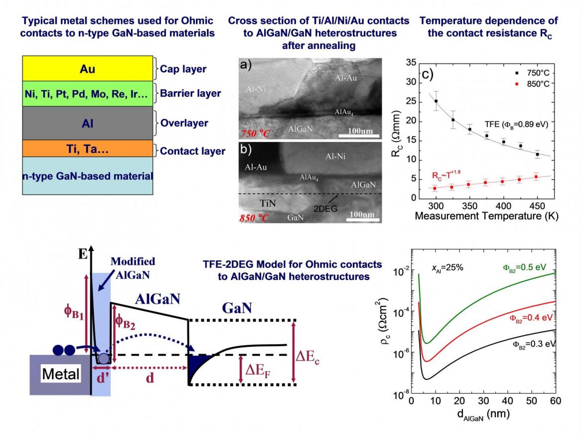
In this review article, a comprehensive study of the mechanisms of Ohmic contact formation on GaN-based materials is presented. After a brief introduction on the physics of Ohmic contacts, a resume of the most important results obtained in literature is reported for each of the systems taken in consideration (n-type GaN, p-type GaN and AlGaN/GaN heterostructures). The optimal metallization schemes and processing conditions to obtain low resistance Ohmic contacts are presented, discussing the role of the single metals composing the stack and the modification induced by the thermal annealing, either on the metal layers or at the interface with GaN. Physical insights on the mechanism of Ohmic contact formation have been gained by correlating the temperature dependence of the electrical parameters with a morphological/structural analysis of the interface. In the case of the AlGaN/GaN systems, the influence of the heterostructure parameters on the Ohmic contacts has been taken into account adapting the classical thermionic field emission model to the presence of the two dimensional electron gas (2DEG). Finally, the state of the art of “Au-free” metallization to AlGaN/GaN heterostructures is also presented, being this latter a relevant topic for the integration of GaN technology on large scale Silicon devices fabs.