
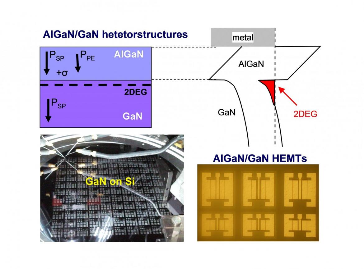
Gallium Nitride (GaN) and its related AlxGa1-xN ternary alloys have excellent properties (like a wide band gap, a high critical electric field and a high electron saturation velocity) making them suitable semiconductors for high power and high frequency devices. In particular, due to the presence of the two dimensional electron gas (2DEG) generated by the spontaneous and piezoelectric polarization charges, AlGaN/GaN heterostructures can be used for the fabrication of high electron mobility transistors (HEMTs).
The research activity carried out at IMM Catania headquarters is focused on fundamental aspects related to lateral and vertical GaN-based devices, i.e., spanning from the development and characterization of the elementary device building blocks (contacts, gate dielectrics, etc.), to their integration and impact into the device behavior, considering also the role of the material quality. The involved team holds a multidisciplinary background (physics, chemistry, electronic engineering and material science) and expertise on GaN materials and devices.
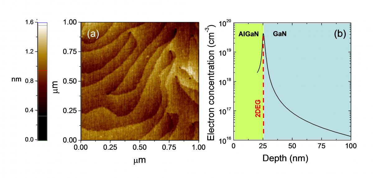
The work is performed on a variety of substrates including large-area Si, SiC, and sapphire, with a view towards “free-standing” GaN for novel vertical devices concepts. The incoming GaN-based epilayers and AlGaN/GaN heterostructures are characterized in terms surface morphology, electrically active dislocations density, sheet carrier density and mobility of the 2DEG, etc. The activity includes not only the physical characterization of materials and processes, but also the fabrication of devices and test patterns (i.e., Schottky, MIS capacitors, TLM and VdP, HEMTs, MISHEMTs, ...) for advanced electrical analyses.
The main topics currently under investigation include:
- Ohmic and Schottky contacts to AlGaN/GaN HEMTs, GaN diodes and p-GaN materials
- Interfaces of dielectrics with GaN and AlGaN for MOSHEMTs
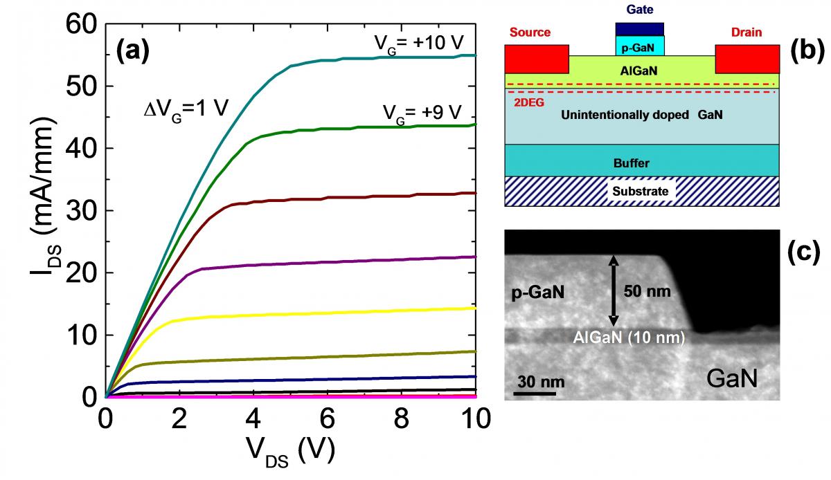
- Processing approaches for normally-off HEMTs (recessed gate, p-GaN gate, etc.)
- Synthesis and characterization of novel dielectrics and nano-laminate materials by Atomic Layer Deposition (ALD)
- Vertical Schottky diodes based on free-standing GaN
In the last years, the activity resulted into extensive studies on contact technology for GaN-based materials, correlating the current transport mechanisms with the contacts microstructure and material quality. In this context, the role of the metal gate and annealing processes on the characteristics of normally-off HEMTs with a p-GaN gate has been also clarified. Activity on the synthesis, characterization and integration of dielectrics and nano-laminates, whose properties can be tailored by varying the ALD growth conditions, is also carried out to limit gate leakage and current collapse effects in GaN devices.
The group has several national and international collaborations with industrial and academic institutions.