
INTRODUCTION
| This laboratory is dedicated to isotropic and anisotropic etching of thin films a by wet and dry processes. Here are located also the facilities for substrate and photolithographic mask surface cleaning. |
| Film growth | |
|
|
PECVDPlasma Enhanced Chemical Vapour Deposition system are used to deposit thin film of:
|
| Deposition | |
|
|
Pentacene EvaporatorPentacene thin films are obtained in high vacuum chamber (pressure 10-7 mbar) having 200C Radak source. The pentacene purity is 99,9%. |
|
|
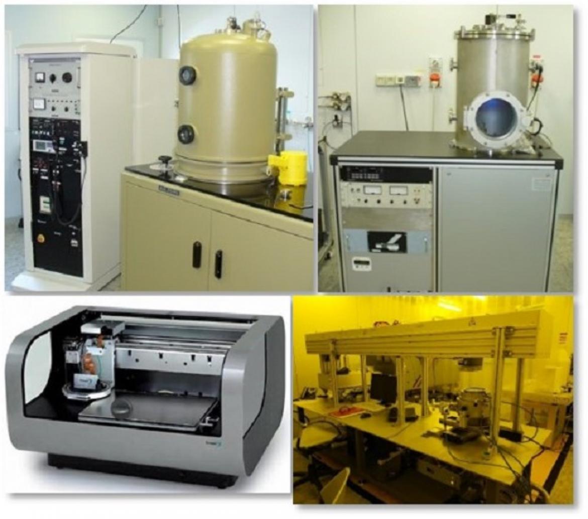
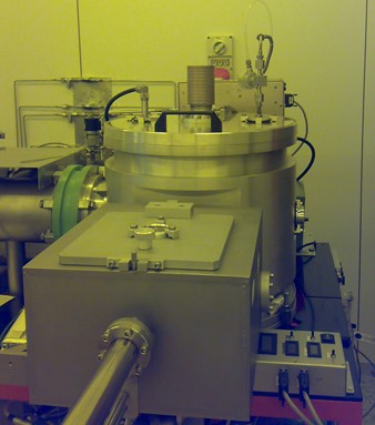
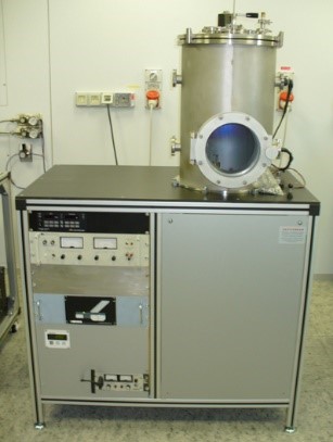
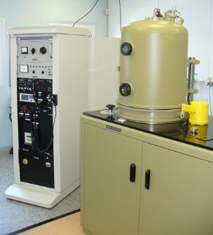
Balzer 510 evaporation systemThe Evaporation System has an electron beam and a thermal evaporation sources. The ultra high vacuum is obtained by a cryopump APD Cryogenics. Mainly used for thin film metal evaporation (Cr, Ti, Au, Ni, Pd, etc) and then for dielectric (SiOx). It is equipped by a Inficon Quartz for thickness and depo rate control. |
|
|
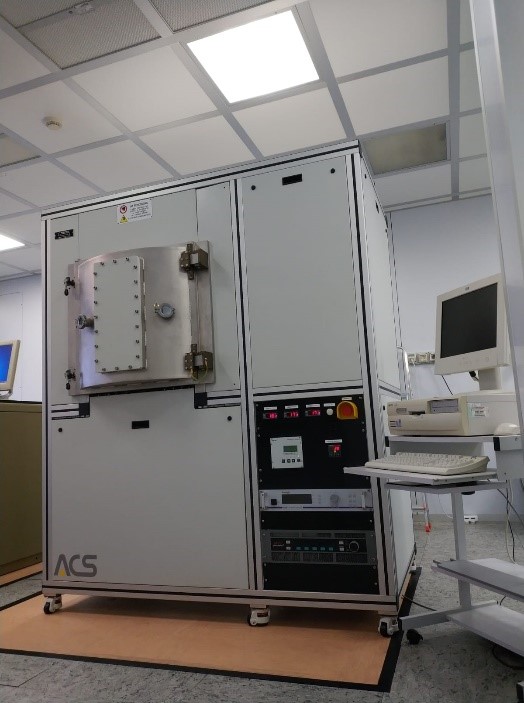
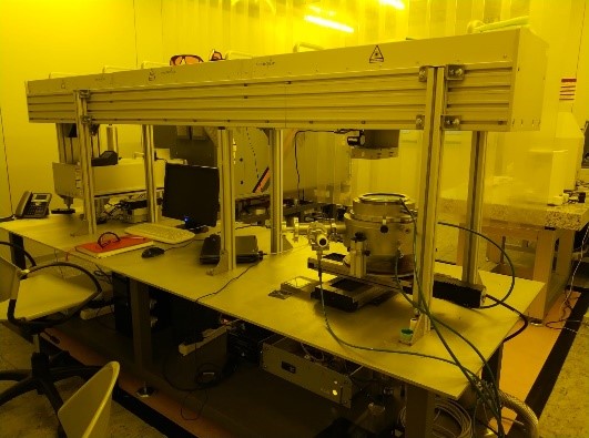
VS-40 Sistec SputteringSputtering Sytem equipped with three catode (actually Titanium, Alluminum and Cromium target mounted) able to perform RF and DC sputtering deposition. The pumping system consists in rotary pump and turbomolecular one. The system is able to process up to 12 four inches wafers during the same run and is equipped by a Pfeiffer mass spectrometer. |
| Printing system | |
|
|
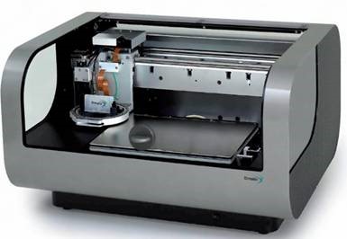
Dimatix is a laboratory benchtop digital ink jet printing system.
|
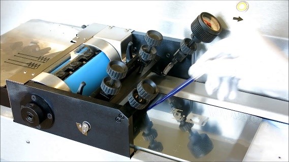 |
Labratest Gravure printing systemLabratester gravure printer is a laboratory printing machine ideal for testing gravure and functional inks and for R&D and pilot applications.
Its main characteristics are:
|
| Thermal processes | |
|
|
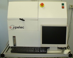
Rapid thermal annealingThe RTA is used to heat a silicon wafer to a sufficiently high temperature so that the silicon lattice is reformed. Rapid heating and cooling of the wafer also minimize the effect of particles diffusion. By varying timeand temperature settings on RTA dopant diffusion can be controlled in order to move dopants to a specific depth. |
|
|
Excimer laser annealingThe excimer laser light (308 nm) is very efficiently absorbed in an ultra-thin amorphous silicon surface layer without heating the underlying substrate. The homogenized excimer laser beam is scanned across the surface. Within the laser pulse duration (approx. 30 ns) the amorphous-silicon layer is rapidly heated and melted. As it cools down the re-crystallization into poly-silicon occurs. Excimer laser induced crystallization of amorphous silicon (a-Si) to low temperature poly-silicon (LTPS) is a pivotal technology for high performance TFT devices, offering excellent resolution and brightness, large angle of view, high pixel refresh rates, and the possibility of display driver circuitry integration on the panel for the next step in the ongoing miniaturization process. |
| Micro/Nano fabrication |