
Light detection will be attempted by using Si and Ge quantum structures embedded in insulating matrices or by low-cost synthesized ZnO nanostructures.
The first activity is focused on the synthesis and characterization of Si-based thin films containing Si or Ge quantum dots or quantum wells for tuning and increasing the efficiency of the light detection. These materials are grown by PVD, or CVD or colloidal solutions in order to exploit different capabilities and costs for the fabrication of detectors. Both amorphous and crystalline nanostructures embedded in SiO2 or Si3N4 are prepared on Si and quartz substrates, depending on the type of application and characterization to be performed. This activity has a strong overlap with that dealing with the energy conversion devices. The innovation is represented by the use of the quantum confining effects in the nanostructures to increase and to control the optical bandgap and the spectral absorption efficiency of the material. The proof of concept has been reported by fabricating a very simple prototype made of a SiO2 film with Ge quantum dots grown on n-type Si wafer, with a TCO front contact, under external bias. Potential applications are ultra-thin detectors in the Visible and IR spectral range.
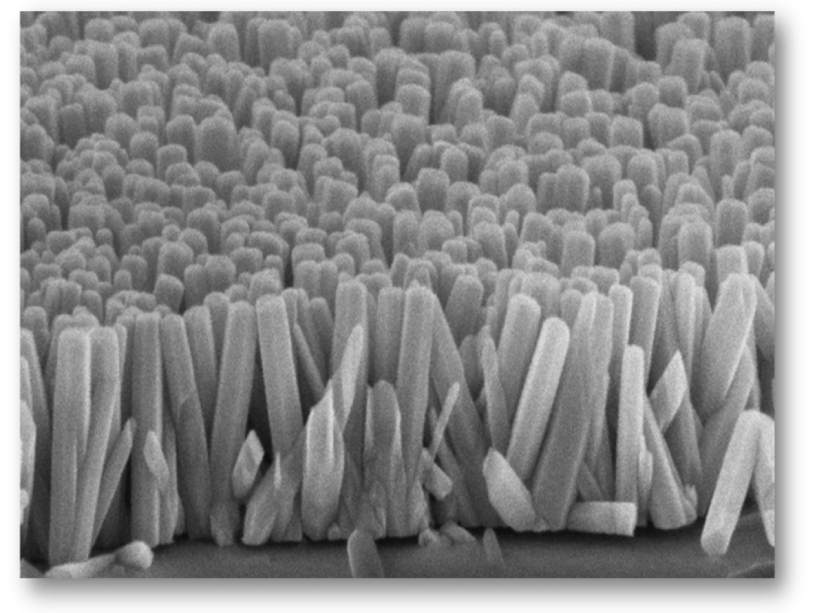
UV sensing will be performed by using ZnO nanostructures as chemistores whose resistivity changes after UV illumination. Novel ZnO nanostructures, defect engineering and Au nanoparticles will be used to improve the selectivity (blindness to visible), sensitivity and response/recovery time of prototypal devices.