
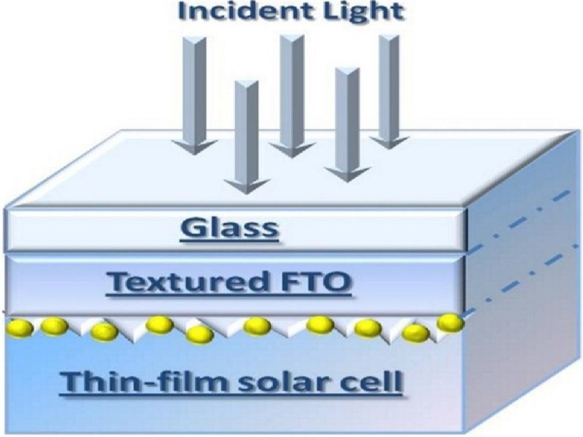
The interest in assembling metal nanoparticles (NPs) onto conductive transparent substrates, as fluorine doped-tin-oxide (SnO2:F, FTO), has increased as the resulting interfaces show interesting optical properties exhibiting structure-dependent transmission/absorption spectra due to the occurrence of localized surface plasmon resonance effects (LSPR) that could be successfully used in plasmonic solar cell to increase the energy conversion efficiency. In this sense, Au and Ag NPs were highly studied since they exhibit extraordinary optical resonances: when excited by an electromagnetic radiation, they exhibit LSPR due to the collective oscillations of their conduction electrons. More recently, however, also Pd and Pt NPs have proved to be efficient plasmonic structures and, more than Au and Ag, Pd and Pt NPs are very promising for catalysis, photocatalysis, and energy storage applications. In our previous works [1, 2] we fabricated a prototype of Si-based thin film plasmonic solar cell by growing a p-i-n Si structure on a textured FTO/glass substrate and placing Au NPs at the p-i-n/FTO interface (see Fig. 1) to exploit their plasmonic characteristics (see Fig.2).
Fig. 1- Representation of a plasmonic solar cell prototype. In the glass/FTO/ metal NPs multilayer, the large fraction of radiation transmitted by the transparent layer interacts with the metal NPs used as sub-wavelength scattering elements to trap the sunlight into an absorbing semiconductor thin film.
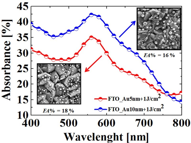
Fig. 2- Comparison between the absorbance values of the substrates covered by 5 nm (red curve) or 10 nm of Au (blue curve) and submitted to laser treatment at higher energy. The values of the filled area (FA%) and the unlike Au NPs sizes justify the differences in the absorption spectra.
In the present activity, we aim to extend our study to Pd and Pt NPs. So, our idea is to deposit Pd and Pt thin films on the textured FTO surface and to induce Pd and Pt NPs formation by laser annealing processes. Using microscopic analyses we will connect the size and surface density of the produced NPs to the process parameters (thickness of the starting Pt or Pd films and laser fluence), see the first results in Fig. 3 [3].
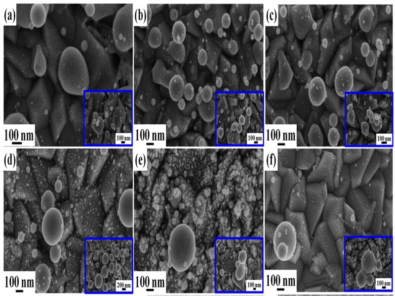
Fig. 3- Microscopies of the Pd NPs formed on the FTO surface after laser irradiations of the deposited films. (a)-(c) 17.6 nm-thick Pd film irradiated by 0.5 (a), 1.00 (b), and (c) 1.5 J/cm2; (d)-(f) 27.9 nm-thick Pd film irradiated by 0.5 (d), 1.00 (e), and (f) 1.5 J/cm2.
Then, we will analyze, by absorption, transmittance and reflectance measurements, the optical properties of the produced arrays of Pt and Pt NPs on the basis of their structural characteristics. Finally, we will test the performance of these structures in prototypes of plasmonic solar cells and electrochemical devices.
[1] F. Ruffino, et al., J. Mater. Sci. 49, 8498 (2014).
[2] F. Ruffino, et al., Funct. Mater. Lett. 8, 1550017 (2015).
[3] F. Ruffino, et al., Physica E 83, 215 (2016).