
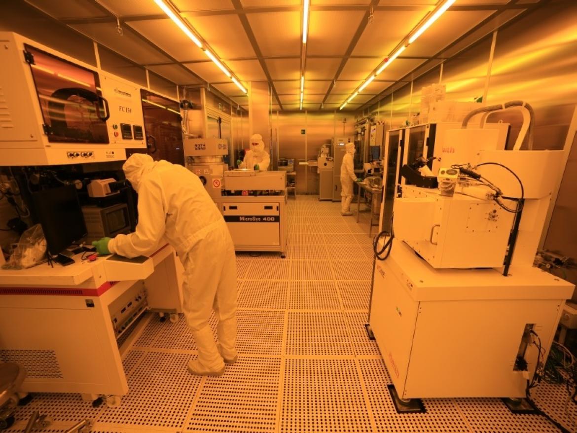
The class 10 (ISO 4) clean room area (100 m2) at IMM HQ is equipped with micro- and nanofabrication facilities, employed to develop new and/or unconventional processes and to fabricate device prototypes (both on small samples and on wafer-scale) on Si and on novel/advanced materials (SiC, GaN, 2D materials,…).
|
OPTICAL PHOTOLITHOGRAPHY |
|
Laser beam direct writing lithography (Reference persons: S. Di Franco, F. Roccaforte) The Laser beam direct writing lithography from is equipped with a laser diode (wavelength 405 nm) and a high resolution pattern generator (up to 0.5 µm with 2 mm write-head). It can be used for low volume mask making or direct exposure of microstructures on basically any flat material coated with photoresist. The system allows to process samples of different size (from small pieces, 10 mm × 10 mm, up to 150 mm wafers) and arbitrary shape.
|
|
|
|
NANOLITHOGRAPHY |
|
Electron beam lithography (Reference person: Giuseppe D’Arrigo)
The E-Line apparatus by Raith has the following characteristics:
It is also equipped with:
|
|
Nanoimprint lithography (Reference persons: S. Di Franco, F. Giannazzo) The fromis a nanoimprinting lithography system, equipped both with the harm for “hot-embossing lithography” and for “UV-NIL”. It allows handling chip-size up to 40 mm and substrates up to 150 mm in diameter. Furthermore, it is equipped with a very high positioning accuracy stage (sensitivity ~1 mm), with optical alignment system. An apparatus for automatic polymer deposition is present. Temperature ramps up to 400°C with heating speed up to 10 °C/s and sensitivity of 1 °C, and forces up 50 N can be applied during imprinting. Thanks to the high optical alignment resolution, samples positioning accuracy, controlled temperature and pressure ramps, this system has been employed also for high precision thermo-compression printing of novel materials (such us graphene and transition metal dichalcogenides) to a target substrate. |
|
|
|
ETCHING EQUIPMENTS |
|
Inductively coupled plasma etching (Reference persons: S. Di Franco, F. Roccaforte) The is system for plasma etching of different materials (e.g., Si, SiO2, Si3N4, GaN, SiC, AlN) with substrate size up to 12 inches. The system includes a cylindrical vacuum chamber, a helium back side coolable carrier to substrate handling, pumping system, plasma generation and a spectrometer to detection etching end point. A separate load-lock and pumping system allows the automatic loading and unloading of the substrates to the process chamber. Several reactive gases are used, such as chlorine, borane trichloride, sulfur hexafluoride and trifluoromethane. |
|
|
|
GROWTH, DEPOSITION AND THERMAL PROCESSES |
|
Metal sputtering system (Reference persons: S. Di Franco, F. Roccaforte) The Q300T D Dual Target Sequential Sputtering System from Quorum Technologies is a fully automatic, large chamber, dual-head sputter coater, suited for many thin film applications and device fabrication. The dual-head configuration allows two different metals to be sequentially sputtered without the need to 'break' vacuum. Thin films depositions can be done both on small samples and on entire wafers up to 150mm in diameter. The system is equipped with a fully automatic touch screen control and a dual channel film thickness monitor module. The pressure in the chamber during deposition can be automatically set. A wide range of metals can be sputtered with the Q300T D (Au, Pt, Ni, Cr, Ti, Al, Ta, Mo, …).
DC Magnetron Sputtering (Reference person: A. Alberti) DC magnetron sputtering system made by Kenotec (today Kenosistec). The high vacuum chamber (10-9 Torr) is equipped with three metallic cathodes for sequential deposition of multilayer structures on 6 inches wafers, and with a station for etching procedures. It is currently used to deposit from thin (about 1 nm) to thick (larger than 1 µm) layers of nickel, cobalt, aluminum and titanium for applications in microelectronic devices such as MOS-transistors and Schottky diodes. The system is equipped with two additional inlets for oxygen and nitrogen injection into the deposition chamber for reactive deposition of nitride and oxide such as TiN and TiO2 mainly used in microelectronics, photovoltaics and sensors architectures. In situ heating during deposition up to 250°C can be also applied by an integrated stage.
Inductively Coupled Plasma CVD (Reference person: G. Mannino) This type of deposition improves considerably the capabilities of depositing a layer by decomposition of precursors gas in plasma by coupling an inductive RF. Thanks to this approach one can have higher ionized species in the plasma up to one order of magnitude with respect to conventional plasma systems. This allows to reduce the deposition temperature down to room temperature producing layers on any substrate (including polymeric and glass substrates) with excellent electro-optical properties. Furthermore, the vertical and cylindrical configuration of the chamber allows maintaining the sample outside the plasma region ensuring no acceleration of charged species toward it. The sample surface is therefore is not damaged and better preserved. The system actually in use allows to deposit several material types (Si or C based) by these precursors: SiH4, CH4, N2, N2O, PH3, TMB, NH3.
Atomic Layer Deposition (Reference persons: R. Lo Nigro, S. Di Franco) The Atomic Layer Deposition reactor PE ALD LL SENTECH Instruments GmbH enables the controlled deposition of ultra-thin conformal, pinhole- and particle-free films with excellent uniformity for a wide range of materials, including high-k dielectrics (Al2O3, HfO2), nitrides (AlN) and nanolaminates (Al2O3/HfO2 stacks) by thermal as well as plasma enhanced processing. Depositions can be performed on 2, 4, 6 and 8 inches wafers as well as on small pieces having different sizes and shapes. Substrate stage and reactor wall temperature can be controlled up to 500°C and 150°C, respectively. Deposition processes of high-k dielectrics on wide-bandgap semiconductors (SiC, GaN) and 2D materials (graphene, MoS2) have been developed with this equipment.
Furnaces
The laminar flow furnace by EATON allows annealing of silicon wafers up to 8 inches at temperatures up to 1250 °C in O2, N2 or Ar gas ambient.
The Jetfirst150 by Jipelec is a lamp rapid thermal annealing (RTA) furnace for thermal processes at temperatures up to 1250 °C and heating ramp rate up 150 °C/s. Processes can be performed in N2, Ar or O2 flow. It allows annealing of small samples and wafers up to 6 inches.
The Carbolite horizontal furnace is equipped with an Al2O3 tube (75 mm internal diameter, 120 cm long). One or more samples can be loaded into a floating quartz boat. Thermal processes can be carried out in N2, Ar or O2 ambient up to a temperature of 1400 °C.
A horizontal tube Furnace by Lenton LTF12/75/750 is installed in the Laboratory for C-based nanomaterials and allows to perform thermal treatments in vacuum or in gas environment, with a maximum temperature of 1200°C. Four different process gas lines are connected: CH4, H2, N2 and Ar. It is possible to use one gas or to mix more gases in a controlled ratio.
The vacuum oven A7V10WS0000 by Mazzali allows annealing of silicon wafers up to 8 inches at temperatures between 40°C and 250 °C in vacuum (0.1mbar), air or N2. Annealing times can be varied between 2 and 50 hours.
Laser Annealing (Reference person: G. Mannino) Semiconductor laser ensures high power in few milliseconds annealing. This equipment takes the advantage typical of laser systems of heating materials with high ramp rates, up to 106 °C/s, but allows a careful control of the annealing temperature below the melting point. This results in effective crystallization of micron-thick amorphous Si layers and synthesis of Si nanocrystals for solar cells, full crystallization of hydrogen rich a-Si layers without void formation or film degradation and formation of highly active doped junction with no appreciable dopant diffusion. The system source is a CW 600 W GaAs diodes array which is focused on the sample reaching a maximum power density of 300 kW/cm2 and two step by step motors to control annealing time from 1 to 170 ms on wafers up to 8 inches. |
|
|
|
MICROSYSTEM PROCESSES |
|
Micro-Nanomachining and Electrochemical Lab (Reference persons: G. D’Arrigo, A. Sciuto) The Micro-Nanomachining lab is equipped with:
An UV-light Curing and Single Binary Mask exposition flood system Dymax 2000 for the processing of large area samples up to 200x200 mm2, with UV intensity up to 225 mW/cm2 and with shutter actuated manually or by PLC. |
|
|
|
ION IMPLANTATION |
|
Tandem (Reference persons: A. Marino, A. La Magna) The linear Tandetron accelerator is capable to produce a large variety of highly stable ion beams of virtually all periodic-system elements (hydrogen and noble gases apart) with an energy from 30 keV up to 10 MeV (depending on element and state of charge) for materials modification and analysis. A source-selection/analyzing-switching magnet (with a mass-energy product of 24 AMU-MeV) is used to mass analyze the ion beams. The magnet is capable of inflecting and analyzing all ions in the periodic table through either the +30° or -30° input ports. It is possible to obtain an implant surface dimension of 1, 2, 3, or 4 inches of diameter. The targets can be cooled at liquid nitrogen temperature or they can be heated up to 400 °C during ion implantation. It is possible to implant up to 8 inches substrates. |


