
Giuseppe D'Arrigo, CNR-IMM Catania
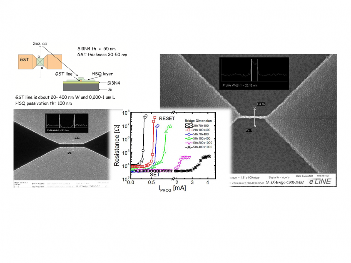
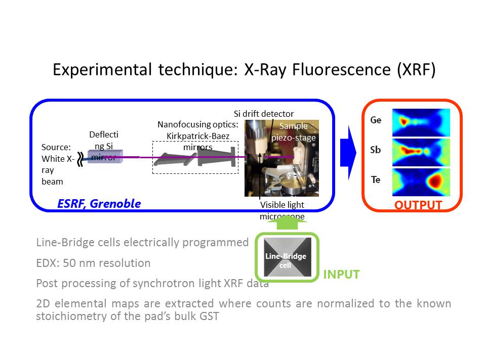
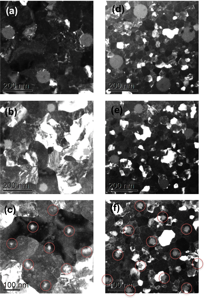
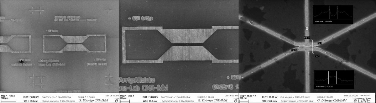
The working principle of a Phase Change Memory (PCM) cell exploits the reversible transition between a crystalline and an amorphous phase and vice versa, both induced by electric pulses of different magnitude and duration. The two phases are characterized respectively by a high (SET) and a low (RESET) conductive state. The transformation between the crystalline and the amorphous phase is induced by a high current pulse able to melt the cell active volume; its subsequent fast quenching (1 to 10 ns) determines the crystal-to-amorphous transformation. The reverse transition requires instead a slower cooling down from the melt (hundreds of ns). Cycling endurance, namely the iteration of SET and RESET operations, is the result of a sequence of melt-quench processes. Cell degradation occurs usually with increasing the number of cycles, e.g. the variation of cell resistance in both states during cycling. The stoichiometry variations were observed in all PCM architectures, mushroom and wall configurations, in pore configurations and in the self-heating structures and are addressable to the high electric field or current density necessary to achieve the melt quenching during the SET and RESET procedures. Resistance cell variation has been correlated by Syncrotone light XRF (Grenoble) and Energy-Dispersive X-ray spectroscopy (EDX) analyses and by TEM analyses to the local change in atomic composition inside the cell active volume, as a consequence of cycling.The stoichiometry variations still represent an argument of discussion because the entity of segregation, the elements distribution in the active volume and the final composition depend on the particular kind of adopted PCM architecture. The driving forces (electrical, thermal, mechanical and chemical) that promote the segregation were studied. The activity is done with MICRON Technology Inc. BOISE, since 2012, under a contract between CNR-IMM and Micron.
AMORPHIZED NANO AREAS in Chalcogenide materials and in Silcon.
The activity was addressed to the retention study on Nanoamorphised GST and for the Silicon nano-amorphisation and doping confinament study. The amorphised nanoareas were fabricated by Electron-Beam Lithography and Ion Implantation technique. The GST amorphous regions in the nanometric scale are embedded in a crystalline environment, quite similar to the RESET configuration i.e. an amorphous dome in the active device region under a thermic stress. Apertures of 20 -50 -100 nm diameter respectively were opened by Electron Beam Lithography in a 100 nm thick PMMA positive resist.
Inovative contacts for Memory applications.
Non volatile memories based on Phase Change Materials, e. g. Ge2Sb2Te5 are considered possible candidates in the present market scenario. The Extreme Ultraviolet Lithography (EUVL) technology, actually, allows to scale the memory device structures in the node of 18-20 nm. The capability of increasing the bits in the storage devices is one of the most important requests of the market for Non-Volatile Memory that remains one of key product segment for the mass production. The scaling possibilities of PCM must be coupled to the need of increasing the device characteristics also in the terms of power performances. The reduction in power consumption for each bit transcription implies also a reduction of the power losses. In the present activity we investigate the physical, mechanical and electrical, properties mechanically transferred CVD-grown graphene layer on different PCM and the possible utilization of graphene as scaled contact.The activity is done in collaboration with Dr. Rita Rizzoli IMM-Bologna.
Contact: Giuseppe D'Arrigo