

The theoretical modelling activities ongoing in the IMM - Rome are strictly related and complementary to the experimental activities currently pursued in this Unit.
Currently, the activities are focused on five different research lines:
- Tunable photonic microsystems
- High Frequency Microsystems
- Large Area Electronics
- Numerical simulation of power devices and RF power devices
- Circuital modeling of solid/liquid interfaces and impedance spectrum
IMM Roma Hardware Resources:
- HPC system: 14 nodes with Xeon processors, 70 cores, 288 GB RAM. Access through batch management system.
- Workstation: Lenovo ThinkStation, single node, dual Xeon Silver processor, 40 thread, 256 GB RAM
Reference Person: antonio.valletta@imm.cnr.it
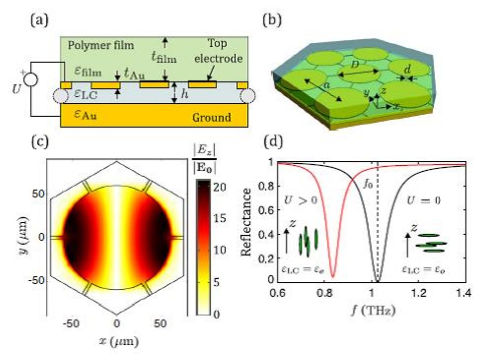
The research activities of the “Tunable photonic microsystems” group of CNR-IMM focus on the design, fabrication, and characterization of novel tunable devices, both integrated and free-space, which target different ranges of the electromagnetic spectrum, from the terahertz to the IR and visible.
The theoretical modeling covers the following topics:
- Electromagnetic wave propagation in both guided-wave and free-space THz, photonic, and plasmonic structures.
- Liquid-crystal orientation and switching studies in confined geometries.
- Time-domain simulation of electromagnetic structures comprising dispersive and anisotropic materials.
The software tools employed include:
- COMSOL Multiphysics®
- RETICOLO: Rigorous Coupled Wave Analysis for gratings (in Matlab).
- FlexPDE: Finite-element model builder for PDEs.
- Finite-difference time-domain built-in codes (in Matlab)
- CUDOS MOF Utilities (Multipole Method for holey fiber analysis).
Reference Persons: romeo.beccherelli@imm.cnr.it
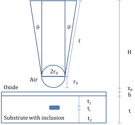 |
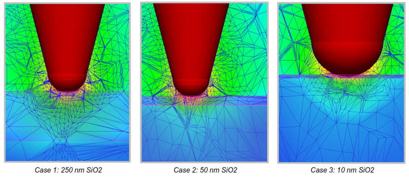 On the left: Geometry used for modelling the tip-sample interaction. The end of the tip is approximated by means of a spherical shape. On the right: Diagram of the interaction between a SMM tip and a silicon oxide layer on the top of a silicon wafer, studied by means of EMPro. The dimension for the end of the tip is r0=100 nm |
The design and theoretical modelling activity performed by the Research Unit involved in the development of High Frequency Microsystems is devoted to:
- the prediction of the frequency response of microwave and millimeter wave configurations
- the phenomenological modelling of devices, including physical mechanisms related to mechanical and thermal properties as well as to charging effects
- the extraction of equivalent circuits to be used as building blocks in complex configurations
In the above framework, different structures have been modeled and are currently studied, depending on their applications.
In the case of High Frequency Signal Processing, devices like resonators, filters, phase shifters, delay lines and antennas are simulated by means of 2D and 3D electromagnetic software packages. The main commercial products used for this purpose are Microwave Office, COMSOL, CST and HFSS. Circuit extraction is performed following an analytical approach, helped by products like MATLAB and MATHCAD, especially when non-conventional materials and configurations are considered. Parameter extraction of metamaterial structures, to determine the effective permeability and permittivity, is a typical example.
Another activity in theoretical modelling is related to Microwave Microscopy Techniques, to study the interaction of micro- and nano-antennas implemented in a Scanning Microwave Microscope (SMM) with the surface of a solid sample and its buried details in the sub-micron range. The calculation of the impedance change due to the interaction is helpful for determining dielectric and magnetic properties of the sample and for imaging purposes. Solid and liquid samples, even with embedded micro- and nano-particles are simulated and analytically modeled.
Reference Persons: romolo.marcelli@imm.cnr.it
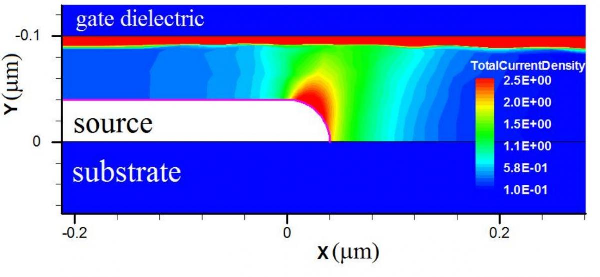
In IMM Rome Unit there is an ongoing research activity focused on the theoretical modelling of large area electronic devices that trace back to the early 90’s, with thorough investigation on the physics of amorphous and polycrystalline silicon thin film transistors (TFT). Currently, the theoretical research activity is mainly focused on the physics and modelling of organic thin film transistors obtained by printing techniques, that are among the technologies candidate for ubiquitous electronics.
Electronic circuits fabricated by using large area compatible processes frequently employs materials with characteristics deeply different from those of the well-known materials used in crystalline silicon applications. The resulting devices have electrical characteristics that are often substantially different from their crystalline silicon counterpart, due to the different device physics associated to the specific materials and processes used. A successful circuit design requires a precise modelling of the device characteristics in all regimes of operation in addition to the availability of compact models that can be efficiently used in circuit simulation software environments. Hence, in addition to scientific motivations, there are also strong technological and industrial reasons in order to understand the phenomena that cause the device characteristics to behave differently from those of crystalline silicon devices and develop compact models that mimic that behaviors.
The thematics that are actively investigated are:
- Physics and modeling of contact effects in organic and inorganic thin film transistors (TFT)
- Charge transport mechanisms in organic materials
- Electrical stability and self-heating effects
- Non-quasi-static AC operation of organic TFT
Software:
- Synopsys® Technology CAD
- COMSOL® Multiphysics
- CADENCE® Virtuoso
Active Collaborations: INFN Sez. RomaTRE; SEES -CINVESTAV (Mexico)
Active Projects: Joint bilateral collaboration project CNR-CINVESTAV (Mexico)
Publications
- A. Valletta, A. Daami, M. Benwadih, R. Coppard, G. Fortunato, M. Rapisarda, et al., "Contact effects in high performance fully printed p-channel organic thin film transistors," Applied Physics Letters, vol. 99, Dec 5 2011
- A. Valletta, M. Rapisarda, S. Calvi, G. Fortunato, M. Frasca, G. Maira, et al., "A DC and small signal AC model for organic thin film transistors including contact effects and non quasi static regime," Organic Electronics, vol. 41, pp. 345-354, Feb 2017.
- A. Valletta, M. Rapisarda, S. Calvi, L. Mariucci, and G. Fortunato, "A Large Signal Non Quasi Static Compact Model for Printed Organic Thin Film Transistors," 2016 46th European Solid-State Device Research Conference (ESSDERC), pp. 460-463, 2016
Reference Persons: antonio.valletta@imm.cnr.it, matteo.rapisarda@imm.cnr.it, luigi.mariucci@imm.cnr.it
Numerical simulation of power devices and RF power devices
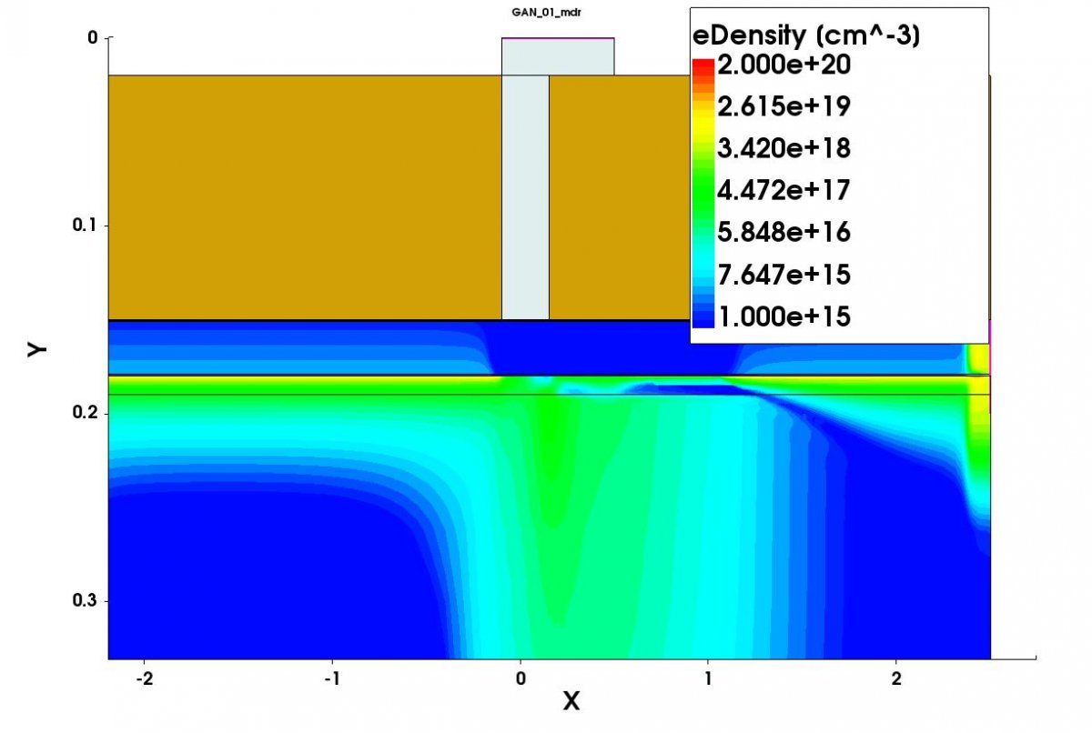
The interest in power devices and RF power devices has received a considerably increase in latest years due to the growing demand of new security and defense systems as well as the expected rise of the electric car market. The realization of such power devices requires accurate designs which depends on the specific characteristics of the materials used as well as their interface properties. Frequently, these devices are realized by using stacks of different materials that separately provides the features required for the correct operation, such as the two-dimensional high electron mobility interface and the heat dissipation layer in AlGaN/GaN hetero structure grown on SiC substrates. Moreover, they often implements advanced architectures that makes difficult to apply “textbook” models in order to predict their characteristics making necessary to resort to numerical simulation in order to simulate the electrical and thermal behavior of the devices.
This activity is devoted to the characterization and simulation of power and RF power devices. Two and three dimensional numerical simulation will be performed in order to gain insights in the interplay between device architectures and their electrical and thermal performances. The results will be used to optimize the device layouts in order to obtain the best trade-off between performances and reliability.
Active Collaborations: Leonardo S.P.A. (ex Finmeccanica)
Active Projects: DISSIPO (funded by regione Lazio, call “Key Enabling Technologies – KETs”)
Reference Persons for this topic: antonio.valletta@imm.cnr.it , luigi.mariucci@imm.cnr.it
Circuital modeling of solid/liquid interfaces and impedance spectrum
Circuital modeling applied to the analysis of (electrochemical) impedance spectra allows to investigate and put in evidence the conduction mechanisms in solid/liquid interfaces and in solid electrolyte materials. In this research activity, we are interested in the modeling of electrochemical biosensors and bulk materials for gas sensing.
Software: Matlab, Mathematica.
Collaborations: Università di Roma Tor Vergata
Publications:
- D. Polese, A. Mattoccia, C. Cavaiola, J. Zoppi, L. Pazzini, G. Fortunato, P. G. Medaglia, L. Maiolo "AC characterization of nitrate intercalated layered double hydroxides gas sensors," 2017 IEEE SENSORS, Glasgow, 2017, pp. 1-3, doi: 10.1109/ICSENS.2017.8234323
- Maiolo L, Polese D, Pecora A, Fortunato G, Shacham-Diamand Y, Convertino A. “Highly Disordered Array of Silicon Nanowires: an Effective and Scalable Approach for Performing and Flexible Electrochemical Biosensors.” Advanced Healthcare Materials . 2016 Mar 9;5(5):575-83. doi: 10.1002/adhm.201500538. Epub 2015 Dec 30. PubMed PMID: 26717420..
Reference Person: davide.polese@imm.cnr.it