
Two-dimensional (2D) crystals beyond graphene are a new frontier in materials science that is currently having a tremendous impact on the nanotechnology of advanced materials. In the present activity attention is paid to the synthesis and physical characterization of two classes of these 2D crystals, emerging 2D elementary crystals including silicene and other Xenes (with X= Ge, Sn or P, known as germanene, stanene or blue-phosphorus, respectively), and transistion metal dichalcogenide (TMD) nanosheets. The concept is to create a portfolio of 2D materials serving as multifunctional platforms for nanotechnology applications (mainly nanoelectronics, but also optoelectronics, nanophotonics, etc.). In details:
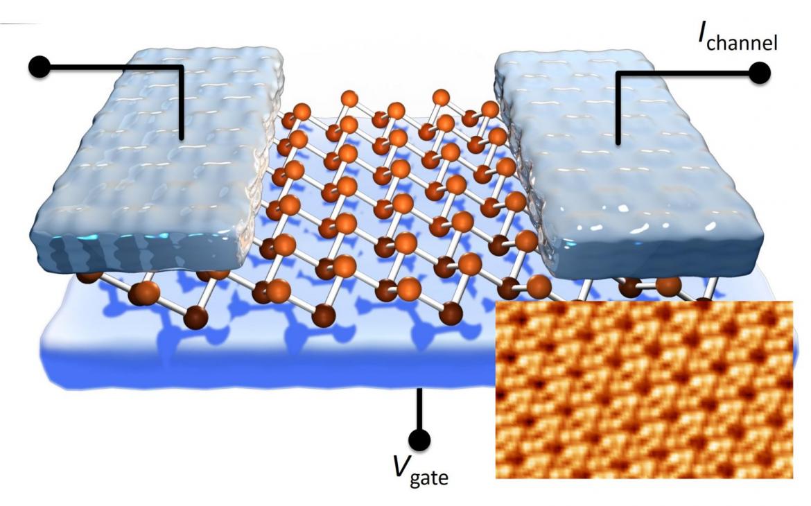
1. Xene: growth and device integration. Xene including silicene, functionalized silicene, stanene, blue-phosphorus will be epitaxially grown on substrates and then integrated on protoypical devices in order to study the electronic and transport properties (see the figure for a pictorial view of a transitor based on a silicene single-layer and atomically resolved topography of the as-grown silicene). Two pathways are followed for device integration: delamination from layered substrates, substrate engineering. In situ and ex situ characterization will be used to validate the grown materials. Post-deposition process will be developed to integrate the Xenes in nanoelectronic device where to study the electrical response.
The goals of the present sub-task are: a) the demonstration of Xene (and functionalized Xene) structures via atom-sensitive probes; b) the integration of the Xene in prototypical device structures.
2. TMD: large-area deposition; defect and anisotropy engineering. TMD will be grown by furnace-based chemical vapor deposition on flat and nanostructured substrates. The procedures developed for the MoS2 growth will be extended to other TMDs (such as SnS2, WS2, and MoTe2) in order to validate the universal character of the methodology and to fabricate van der Waals (vdW) heterostructures. The so-grown layer will be characterized in their structural features, validated as active channels in field effect transistors, and utilized as materials platform for multifunctional applications. The presence of intrinsic and extrinsic defects will be studied in order to manipulate them in functional applications or to induce crystal 2H-1T phase transition. The conformal growth on nanostructured substrate will be also implemented to confer a strongly anisotropic character to the intrinsically isotropic TMD nanosheet thus allowing for the directional control of the optical-electrical properties.
The goals of this sub-actions are: a) grow and characterize large area TMD and their vdW heterostructure with thickness control down to the monolayer; b) Manipulate defects in the TMD nanosheet so as to modulate the doping and to induce 2H-1T phase transitions. c) Growth of highly anisotropic nanosheets.
Contact person: Alessandro Molle