
CMOS technology exploitation is crucial to fabricate in a reliable manner nanodevices where different qubits based on spin degree of freedom can be implemented. One on the goals...
Devices for Information Storage and Processing
Nowadays, micro-nanoelectronic research addresses on one side the continuous scaling of logic and memory devices, also in view of targeting low power electronics and new functionalities. These objectives have been achieved by introducing new materials, exploiting new physical mechanisms and innovative fabrication methods, and with the support of modeling, simulation and design tools. On the other side, there is an increased interest to develop new systems and new computing paradigms, which can address the current emerging societal challenges. For instance, the yearly increasing amount of generated data and the Internet of Thing applications demands for more efficient computation systems in terms of power and capability, to solve problems where the standard von-Neumann based platform fails.
In this framework, the CNR-IMM Institute has a long term and internationally recognized experience in the field of materials, technologies and simulation of logic and non-volatile memory devices. More recently, the Institute has also gained a recognized expertise in developing devices and simulations for neuromorphic and quantum computation paradigms. The institute is currently at the forefront of emerging technologies in the above fields, and the research activities are carried out in collaboration with leading Industries in the field, as well as Italian/international Universities and Research Centers.
The research activities are carried out in different Units of IMM (Agrate Brianza, Bologna, Catania Unit, Catania Headquarters) and are currently focused on the following macro-areas:
-
Materials and advanced devices:
- (i) Resistive type of non-volatile memories, with focus on PCM, nanowire based PCM and oxide-RRAM
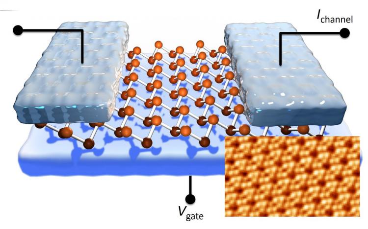
- (ii) Logic devices based on 2D (silicene, MoS2 and other TMDs) and 1D (Si nanowires) systems for low power electronics. Ab initio simulations of 1D and 2D structures.
- (iii) Dielectrics for CMOS and MIM capacitors for power management and analog applications: high-dielectric constant oxides; study of breakdown in dielectrics
- (iv) Materials and devices for spintronics: magnetic tunnel junction, racetrack memory; first principles spectroscopy and simulation of magnetic materials and nanostructures
-
Enabling technologies and advanced characterization methods:
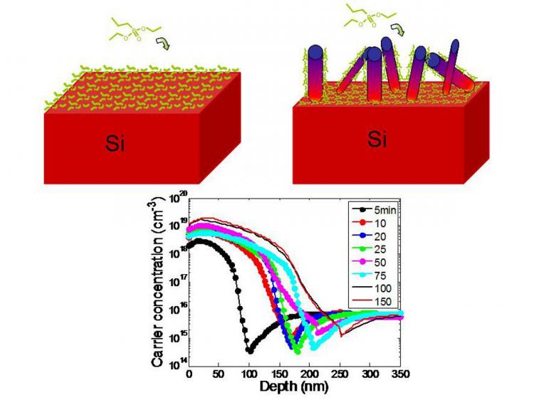
- (i) Development of advanced methods for semiconductor doping
- (ii) Development of advanced nanofabrication tools based on self-assembled materials
- (iii) TEM characterization of nanodevices
-
Towards New Computation Paradigms
- (i) Memristive devices as key elements for neuromorphic systems
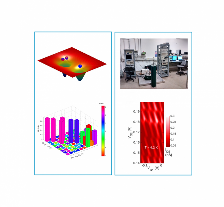
- (ii) Quantum computation systems: modeling/simulation of semiconducting and superconducting Qubit. Characterization of CMOS compatible Si based Qubit. Quantum Cryptography Microsystem.
Coordinator: Spiga Sabina
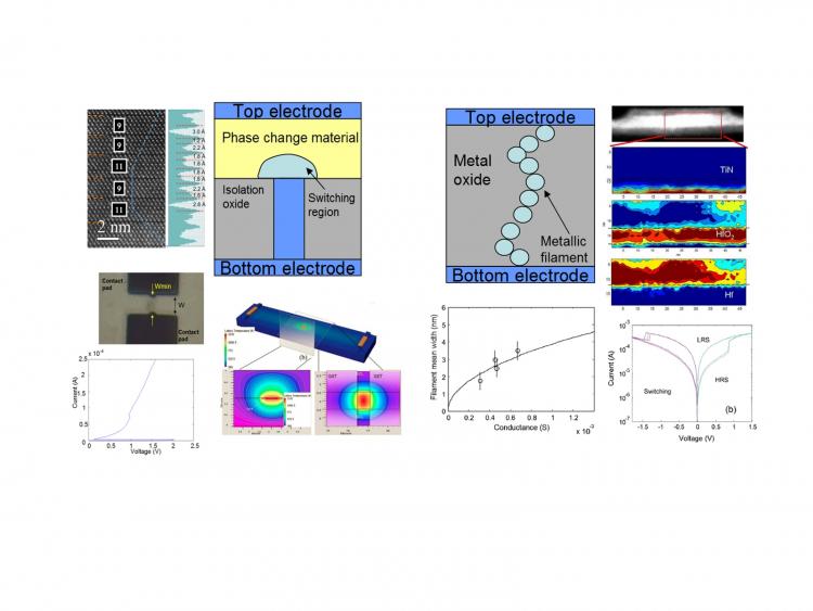
Phase change materials
Phase change materials are interesting candidates for emerging applications in memories, photonics, displays, ovonic threshold switch selectors and non von Neumann...
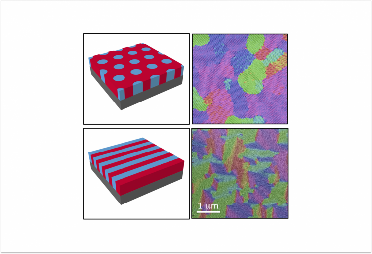
Development of new bottom-up approaches for the synthesis of functional nanostructured materials with typical feature dimension well below 20 nm. The focus of this research...
The demand for low voltage, low power, high performance and increased functionalities has issued severe challenges for the integration progress of nanoelectronic devices so new disruptive...
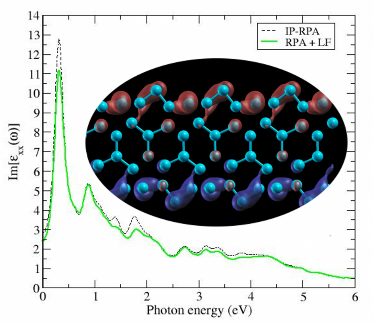
Two-dimensional (2D) crystals beyond graphene are a new frontier in materials science that is currently having a tremendous impact on the nanotechnology of advanced materials. In the present...
Our final target is to determine what are the more promising materials for future ultra scaled electronic that may be based on quantum system: the realization of quantum memory, quantum computer,...
Salvatore Lombardo, CNR-IMM, Catania
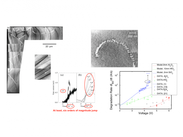
The definition of the basic physical mechanisms of the dielectric breakdown (BD) phenomenon is still an open area of research. In...