PRESS RELEASE: Challenge - New power devices for electric vehicles kicked off!
Challenge project kicked off with a successful meeting on January 23 in Brussels.
Challenge is a HORIZON 2020 project financed under the NMBP (Nanotechnologies, advanced Materials, Biotechnology and Production) work programme that studies growth, processing and devices in cubic silicon carbide (3C-SiC).
3C-SiC technology can have a large impact on the future power device market and is particularly suited for implementation in hybrid electrical vehicles..
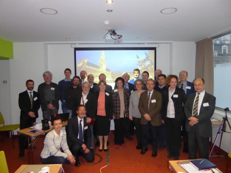
[Brussels, January 23, 2017] Attended by 27 participants from different 7 countries the Challenge project successfully kicked off with a meeting on January 23.
CHALLENGE is a Horizon 2020 project aiming to find an economical solution in response to the needs of a very critical section of the power market; proposing new devices for improving power efficiency in the consumer market between 600V and 1200V. Therefore the 4 year project intends to solve this problem and facilitate the use of a cost effective, low environmental impact new material in the semiconductor family.
Partners are coming from the most advanced public research centres and highly respected Universities on SiC technologies in Europe. The research portfolio ranges from large companies - world leaders in the field and many SMEs from 6 different EU countries in addition to Japan. They will propose a toolbox of solutions for the reduction of defects in bulk cubic silicon carbide material based around new compliance substrates with the ability to develop strategic applications in several fields: from telecommunication to automotive, from consumer electronics to electrical household appliances, from industrial applications to home automation.
The Challenge consortium is unique in breadth across the whole supply chain (equipment, materials, characterizations, processing, power devices, simulations). With the consortiums promise to collect high level research and innovation together with impressive partners’ profiles, this ambitious project can only be brought together with the great support of an EU project.
During the meeting, concrete action plans for the first of this 4-year project were discussed. Topics included hetero-epitaxy stress and defect density, usually observed with these sorts of materials. Crucially the project aims to address the high scalability of this process to 300 mm wafers and the main results required to achieve this goal.
The Kick off meeting was a great opportunity to meet all the 14 partners including 9 private companies and to have a common understanding about the tasks and roles of each and everyone in the project. Moreover partners presented the 6 work packages and discussed some key managerial and financial issues.
Project title:
3C-SiCHetero-epitaxiALLy grown on silicon compliancE substrates and new 3C-SiC substrates for sustaiNable wide-band-Gap powEr devices (CHALLENGE)
Duration: 48 months
Topic: Advanced Materials for Power Electronics based on wide bandgap semiconductor devices technology
Total H2020 grant: 7,997,822 €
For further information, please contact
Francesco La Via
CHALLENGE coordinator
CNR-IMM
Strada VIII 5, 95121 Catania,
Italy
e-mail: francesco.lavia@imm.cnr.it
tel: +39 0955968229