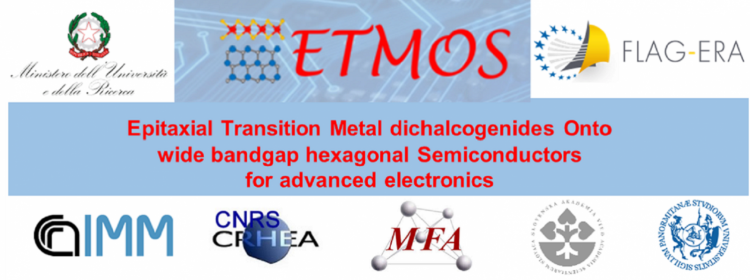
The european project ETMOS, coordinated by CNR-IMM in Catania, has been funded by MUR in the framework of the 2019 FlagERA JTP call "Graphene – Applied Research and Innovation".
The project aims at developing high electronic quality transition metal dichalcogenides (TMDs) onto wide bandgap (WBG) hexagonal semiconductors (SiC, GaN, AlN, AlGaN alloys).
More in details, the specific objectives of the project are:
- The epitaxial growth of MoS2 and WSe2 on different WBG substrates/templates by molecular beam epitaxy (MBE) and pulsed laser deposition (PLD) approaches and, for comparison, by chemical vapor deposition (CVD).
- Multi-scale structural, chemical, optical and electrical characterization and simulations of the grown layers.
- Development of the basic process steps (doping, contacts, dielectrics, etching) on the deposited films and demonstration of device prototypes with TMDs/WBG heterojunctions (including diodes, hot electron transistors, UV photodetectors)
The ETMOS consortium includes 5 partners with complementary skills in thin film growth (CNRS-CRHEA, SAS), advanced characterizations and simulations (CNR-IMM, MFA, Univ. of Palermo), processing and electronic device prototyping (CNR-IMM).
Source:
Date:
2020-04-01 to 2023-03-31