
The theoretical modelling activities ongoing in the IMM - Rome are strictly related and complementary to the experimental activities currently pursued in this Unit.
Currently, the...

The theoretical modelling activities ongoing in the IMM - Rome are strictly related and complementary to the experimental activities currently pursued in this Unit.
Currently, the...
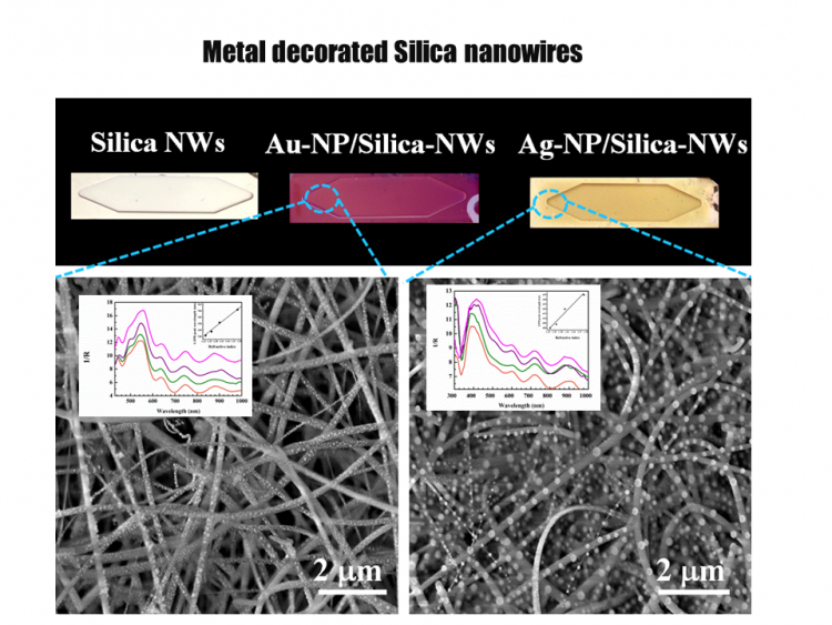
Highly disordered (forest) SiO2 nanowires (NWs), obtained by oxidizing SiNWs, have been decorated with metal (Au, Ag) nanoparticles (NPs). These hybrid structures combine strong scattering...
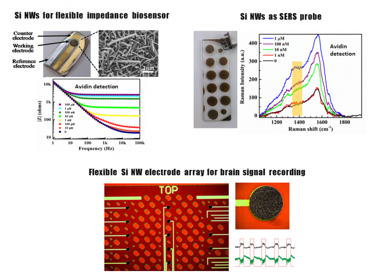
Silicon Nanowires (SiNWs) are expected to play a crucial role in the fields of the biodetection and nanomedicine. Indeed, their unique electronic/optical properties, nanoscale diameter,...
Wearable electronics and pervasive ambient computing are two scenarios where largely distributed flexible sensors networks are expected to be heavily used. The growing demand for sharing large...
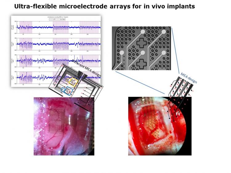
The mechanism by which the neural networks communicate and the understanding of these processes remains the fundamental issue of neuroscience. Long-term brain activity registration and...
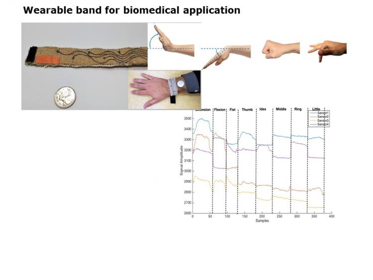
Human gesture monitoring has always been the focus of many academic studies in the biomedical and commercial field. The main challenges are focused on achieving a reliable, high sensitive and...
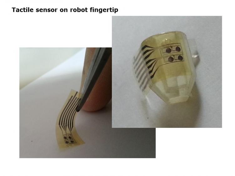
In recent years, a variety of new touch sensing technologies using different materials and transduction methods have been introduced, giving rise to a series of tremendously improved designs of...

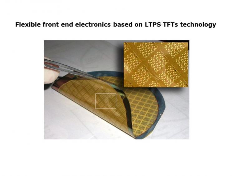
Electronic circuits fabricated by using large area compatible processes frequently employs materials with characteristics deeply different from those of the well-known materials used in...
Organic electronics is an emerging technology that promises to cover a wide range of applications exploiting the intrinsic characteristics of the organic materials: low temperature process,...
We exploit the capabilities of plasma to produce advanced materials for several applications ranging from amorphous solar cells, HIT solar cells, to advanced nanocsryalline materials to be...