
Nickel-Silicon compounds, as most of the transition metal silicides, show peculiar thermodynamic and kinetic behaviours. The large effort devoted to the comprehension of the phenomena governing Ni...
Many efforts of the scientific community working in the field of nanophotonics are currently devoted towards the development of a Si-based light source able to be used for the...
1. Nanoparticles produced by pulsed laser
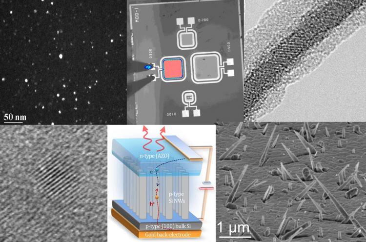
In this activity we will develop Pulsed Laser Ablation in Liquid (PLAL) methodologies to produce metal (Au, Ag (Fig. 1(a))) and metal...
Low-cost synthesis (chemical or electrochemical bath deposition) of nanostructures joins with simple sensor fabrication in lab to exploit the large potentialities of these innovative materials....
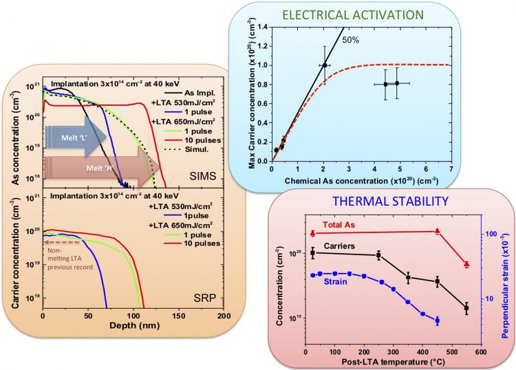
Germanium is experiencing a renaissance during the last decade for several advanced applications such as high- mobility non-Si CMOS transistors to overcome the limits of Si scaling, infrared...
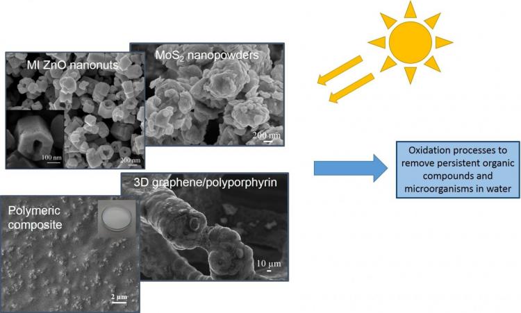
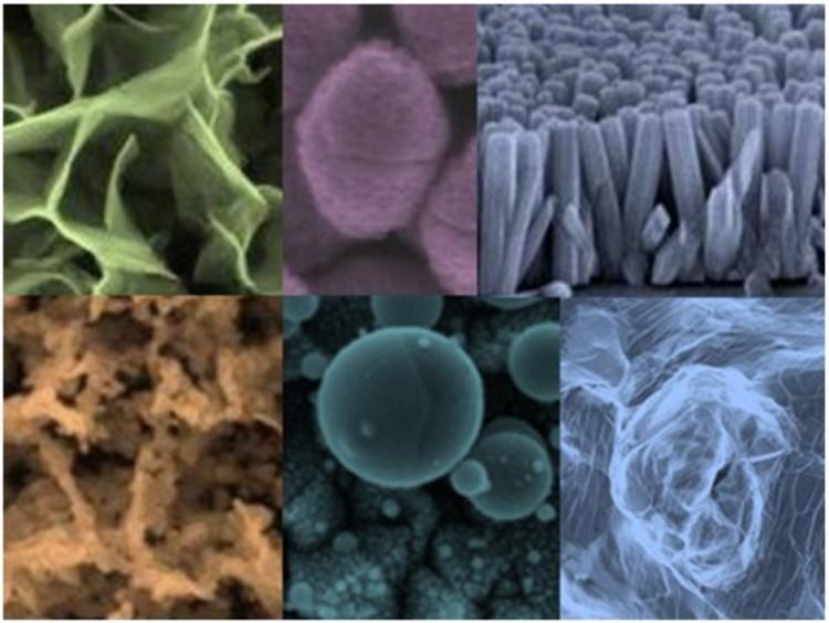
The main concept of the present activity is the synthesis and application of photocatalytic nanostructured materials for water treatment. Nanomaterials are indeed very efficient photocatalysts due...
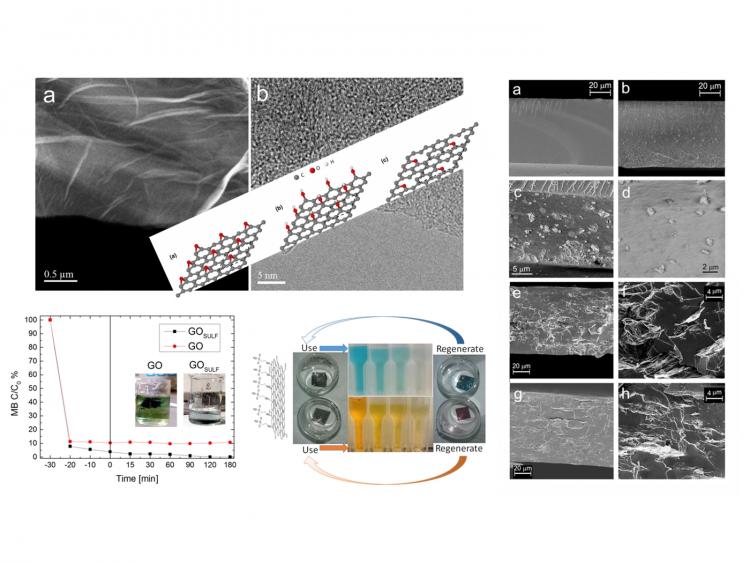
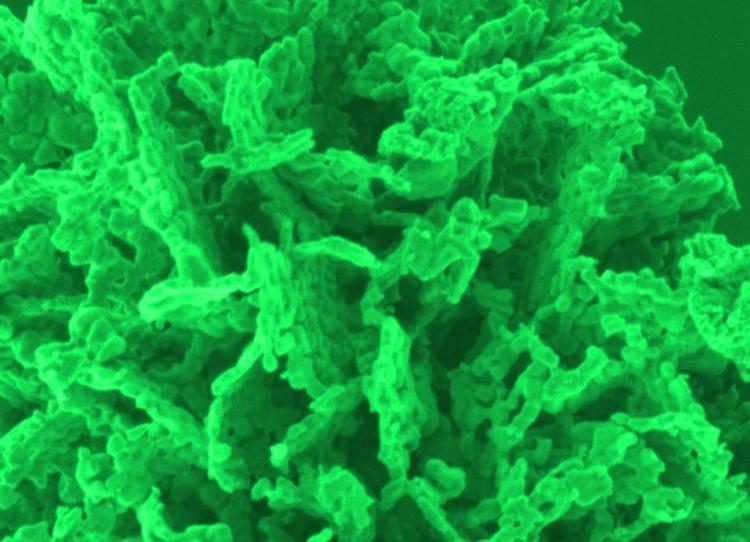
Among the functional nanostructured materials carbon-based nanostructures have an important place in water treatments for purification purposes. Their large aspect ratio and the...
This activity is mainly focused on the synthesis and advanced characterization of materials displaying diverse functionalities. Researchers at IMM Agrate Brianza have a long-standing experience in...
This research activity at IMM Agrate is mainly focused on the use of chemical methods such as atomic layer deposition (ALD) and chemical vapour deposition (CVD) to synthesize materials for...
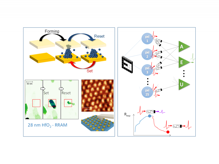
Memristive systems represent today a disruptive technology for the semiconductor industry towards several applications such as data storage (non-volatile memories), non-volatile...