
The synthesis of advanced materials at IMM-HQ has represented the historical core expertise of the Institute Headquarters. It currently avails of the experience of 8 complementary and strongly interacting groups. The several activities of this technological area embrace from the design of materials, processes and advanced applications, to their synthesis, modeling and characterization. In more detail, the activity is based on the use of many leading and state of the art equipments, listed below along with some examples of the materials produced.
Local contact person: Rosaria A. Puglisi
Chemical Vapor Deposition (CVD)
The system is an Inductive Coupled Plasma Chemical Vapour Deposition (ICP–CVD) working at low temperature (typically 70 °C – 200 °C) thanks to a high vertical reactor geometry which ensures a density plasma. It handles up to 8” wafers.
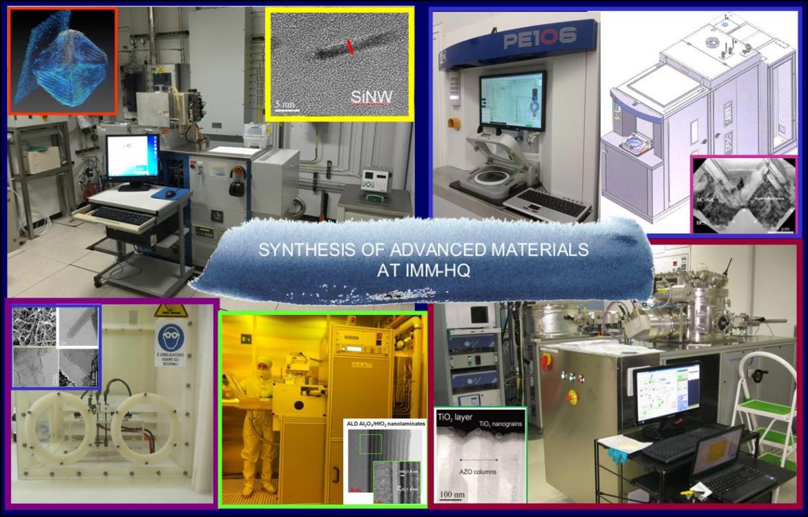
Scope 1. α-Si:H (P or B doped), α-SiC:H, SiOxNyCz, Si & SiC Nanoparticles: We exploit the capabilities of high density plasma to produce at low temperature (<100°C) Si nanostructures, oxynitrides/oxycarbide, SiOxNyCz, SiC and a-Si, eventually doped with P or B, with excellent electro-optical properties for several applications ranging from solar cells to advanced nanostructured materials to be integrated in state of the art devices. Contact Person: Giovanni Mannino
Scope 2. Si nanowires: The nanostructures are synthesized by Vapor-Liquid-Solid growth induced through metal catalysis at temperatures below 400°C and very low gas consumption. They exhibit diameters ≥ 2.5 nm and extremely regular surfaces. Contact Person: Rosaria Puglisi
SiC deposition chamber
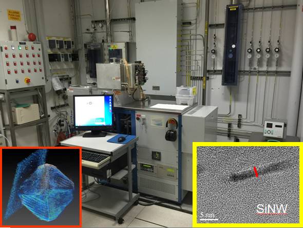
Since 2006, IMM-HQ and Epitaxial Technology Center, now LPE, have founded a Public/Private Laboratory (SiCiLab) with the purpose of developing new reactors, epitaxy processes, characterizations and simulation tools for SiC technology. The new reactor PE106 can grow on 6” wafers, allowing use chloride precursors and high growth rates (100 m/h), with very good thickness and doping uniformity, due to the reaction chamber design developed in IMM-HQ.
Scope. 3C-SiC 4H-SiC Epitaxial growth: This laboratory works essentially on 3C-SiC and 4H-SiC growth and is well known in the world for its activity on very thick 4H-SiC layers for high power devices or detectors for nuclear experiments. Also a very sophisticated 3C-SiC growth process has been developed for MEMS and power devices with very low defect density (SFs, voids, protrusions, …). Contact Person: Francesco La Via
PE ALD
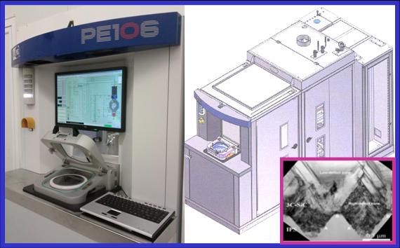
A SENTECH Instruments PE-ALD reactor is present within the clean room of IMM headquarter. Four gasses and three precursor bubblers are available for depositions on 2”, 4”, 6, 8’’ wafers and on small pieces in a 25-500°C temperature range.
Scope. Dielectrics (oxides and nitrides), nano-laminated systems, complex oxide thin films: The system is exploited for the growth of binary oxides (Al2O3, HfO2), nitrides (AlN) and nanolaminated dielectrics. Depending on applications, substrate surface pre-treatments and growth conditions are tuned to optimize the properties of novel gate insulators on wide bandgap semiconductors (SiC, GaN). Moreover, dedicated ALD processes for dielectrics on graphene and other 2D materials (such MoS2) have been developed. Contact Person: Raffaella Lo Nigro
Sputtering
Kenosistec-made reactive sputtering equipment, DC or DC-pulsed. Growth and Reactions can be thermally assisted. Reactive gases: N2 and O2. Deposition methods: co-sputtering or sequential sputtering. Kenosistec-made soft-PVD chamber for photo-active hybrid perovskites deposition
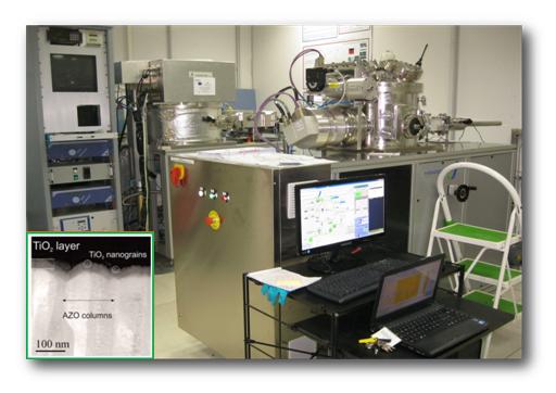
Scope. Metals , Oxides, Nitrides, Silicides; Hybrid perovskites: The system is dedicated to the growth of: Metals (Ti, Ni, Al), Transparent Oxides (TiO2, ZnO:Al, NiO, Al2O3), Nitrides (TiN, AlN), Silicides (Ni-Si, Ti-Si); Hybrid perovskites (e.g. CH3NH3PbI3). Contact Person: Alessandra Alberti
Low-cost chemical and physical synthesis
Drop casting. It is a fast and cheap method to prepare polymeric and hybrid nanocomposite membranes. It consists in dropping a solution containing the polymer and eventual fillers on a flat surface, followed by a spontaneous solvent evaporation.
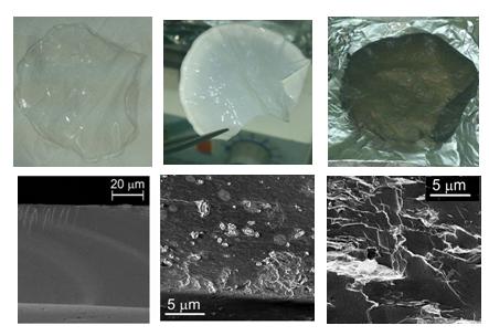
Scope. Free-standing polymeric nanocomposites: Nanocomposite polymeric membranes are produced by drop casting technique. Different kinds of nanofillers (C nanostructures or metal oxides) can be dispersed in the polymeric matrix, allowing to modify the polymer properties, such as hydrophilicity, thermal and mechanical resistance, electrical conductivity, ion and gas transport properties. Contact Person: Silvia Scalese.
Self assembling. The self-assembly process of block copolymers made of PS and PMMA is used to obtain ordered nanoholes on Si suvbstrates. The technique is an easy and cost-effective alternative to standard lithography. Monolayer of molecular precursors, for Si doping, are obtained by dip coating at the boiling temperature of the precursor liquid solutions.
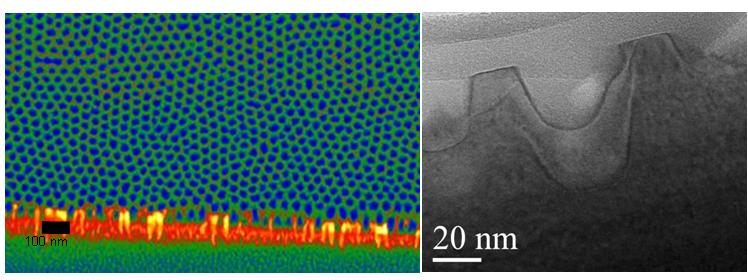
Scope 1. Ordered Si nanopores are fabricated by self-assembling of diblock copolymers. Their size and relative distance range between 10 and 20 nm and can be deterministically controlled by choosing the polymers characteristics and the processing conditions. Contact Person: Rosaria Puglisi
Scope 2. Organic dopant precursors are deposited by solution processing and form a monolayer of molecules over the Si surface allowing to obtain dopant dose of phosphorus or boron of about 1×1015 cm-2. Contact Person: Rosaria Puglisi
Arc discharge in liquid environment. Arc discharge is a low cost synthesis technique based on plasma generation by applying a voltage between two electrodes (graphite rods for synthesis of C nanostructures) in liquid environment (e.g. liquid nitrogen or water): the anode vaporizes and condense in the form of nanostructures on the cathode.
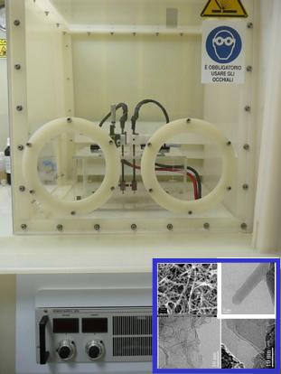
Scope. C-based nanostructures. Carbon nanotubes (CNTs), graphene, graphene oxide (GO), reduced graphene oxide (rGO) are produced by different techniques, such as arc discharge in liquid environment and chemical methods (e.g. chemical exfoliation). The research activity also includes the study of nanocomposites made of carbon nanostructures mixed with metal oxides, produced by co-deposition, electrophoretic methods or laser irradiation of mixed solutions. Contact Person: Silvia Scalese