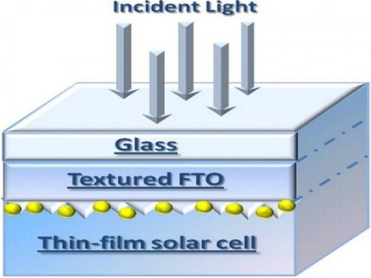
The interest in assembling metal nanoparticles (NPs) onto conductive transparent substrates, as fluorine doped-tin-oxide (SnO2:F, FTO), has increased as the resulting interfaces show interesting optical properties exhibiting structure-dependent transmission/absorption spectra due to th

Development of new bottom-up approaches for the synthesis of functional nanostructured materials with typical feature dimension well below 20 nm.

Design and fabrication of innovative materials and devices for light harvesting.


Third Generation Solar Cells:


Fabrication of high efficiency photovoltaic cells made of:

In the actual Power Devices market, 4H-SiC is the emerging material.

1 Optical lithography (Contact Person: Mario Alia)

2 e-beam lithography (EBL)

Light detection will be attempted by using Si and Ge quantum structures embedded in insulating matrices or by low-cost synthesized ZnO nanostructures.

The aim of this activity is the synthesis and characterization of Si and Ge nanostructures, mainly quantum dots, immersed in dielectric Si-based thin film matrixes (e.g. Si oxides and nitrides).

The use of transparent conductive oxides (TCO) is one of the most critical issues in several fields: photovoltaics, transparent electronics, smart windows, touch screens.

The demand for low voltage, low power, high performance and increased functionalities has issued severe challenges for the integration progress of nanoelectronic devices so new disruptive architectures with 3D schemes have been proposed.

Pages