https://www.mdpi.com/journal/nanomaterials/special_issues/Materials_Elec...
Low dimensional materials (including the wide family of 2D materials, 1D nanotubes or nanowires and 0 D quantum dots) are currently gaining an increasing interest in electronics/optoelectronics, as they allow to extend the performances of traditional semiconductor devices or to demonstrate completely new device concepts and exciting physics.
In this context, combining nanometric spatial resolution with a wide range of physical properties that can be detected, scanning-probe based characterization techniques have proved themselves as essential tools to investigate the structural, electrical, chemical and optical properties of low dimensional systems and their heterojunctions with bulk (3D) semiconductors.
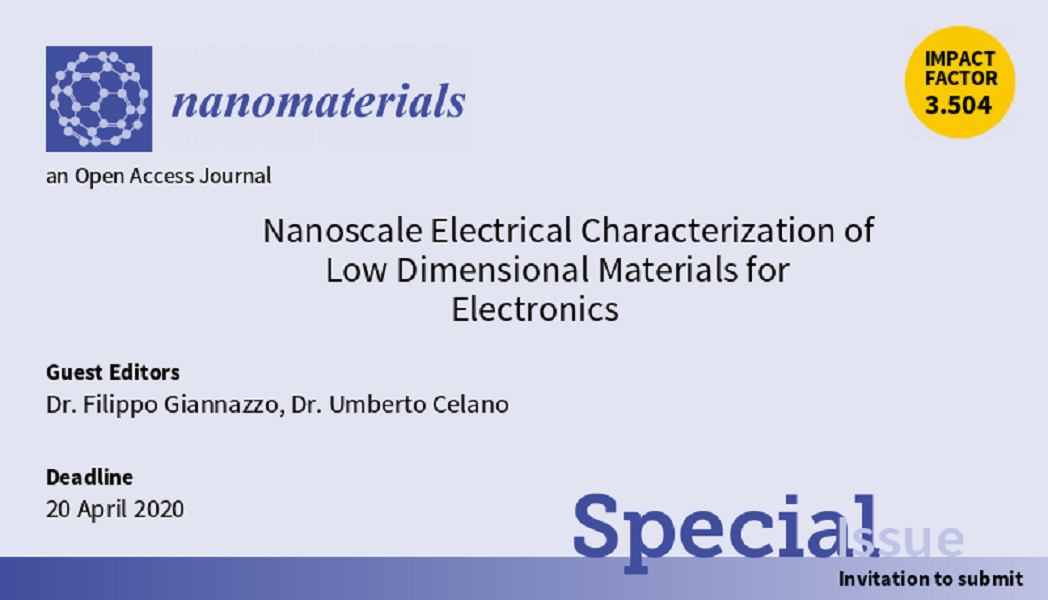
This special issue will be devoted to new developments in nanoscale electrical characterization techniques, and their applications to the analysis of low dimensional materials, including (i) synthesis, (ii) integration and (iii) novel device architectures. The papers collection is open to correlation studies of local electrical/optical measurements with high resolution structural/chemical analyses, as well as to theoretical and modelling works for the interpretation of experimental results in these nanoscale systems.
It is our pleasure to invite you to submit a manuscript for this Special Issue. Full papers, short communications, and reviews are welcome.
Dr. Filippo Giannazzo
Dr. Umberto Celano
Guest Editors
Keywords:
- Scanning probe microscopy
- Scanning Tunneling Microscopy
- Conductive Atomic Force Microscopy
- Scanning Capacitance Microscopy
- Scanning Microwave Impedance Microscopy
- Kelvin Probe Force Microscopy
- Scanning Near Field Optical Microscopy
- 2D materials
- Nanowires
- Quantum dots
Special Issue Guest Editors
Dr. Filippo Giannazzo
Consiglio Nazionale delle Ricerche –Institute for Microelectronics and Microsystems (CNR-IMM), Strada VIII, 5 I-95121 Catania, Italy
Website: https://hq.imm.cnr.it/users/filippogiannazzo
E-mail: Filippo.giannazzo@imm.cnr.it
Interests: graphene, 2D materials, wide-bandgap semiconductors (SiC, GaN), high power and high frequency electronics, scanning probe microscopy
Dr. Umberto Celano
Interuniversitair Micro-Electronica Centrum (IMEC), Leuven Belgium
Website: https://scholar.google.com/citations?user=tmNoFQwAAAAJ&hl=en&oi=ao
E-mail: celano@imec.be
Interests: nanoelectronics, functional nanomaterials, 2D materials, VLSI metrology, scanning probe microscopy