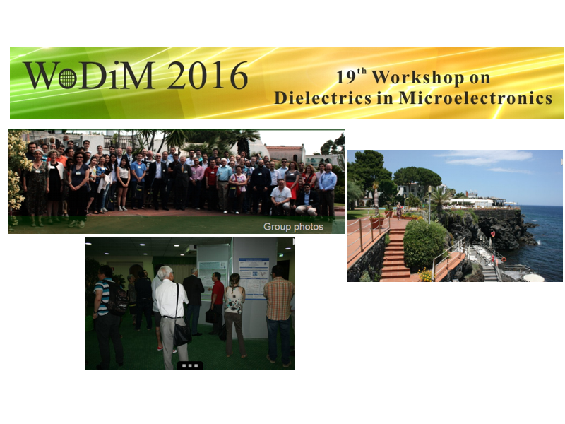
WODIM 2016 has taken place from 27-30 June 2016 at the Hotel Baia Verde, Aci Castello (Catania), Italy. This event was hosted by the Italian National Research Council (CNR) - Institute for Microelectronics and Microsystems (IMM), and celebrated the 10th anniversary of the last time the workshop was held in Italy.
The main objective of the workshop is to bring together specialists who work in the field of dielectrics and all aspects of their application in the field of micro and nanoelectronics. The forum is intended to provide an overview of the state of the art in this significant field, and to promote a relatively informal atmosphere for the discussion of the latest research results. The workshop deals with a range of issues in the field of advanced and new dielectrics, such as: growth and deposition, modelling and simulation, physical and electrical properties, reliability and dielectric applications.
The Workshop concerns the following areas:
- Advanced dielectrics on Si, III/V and Ge for advanced CMOS: High-k/metal gate stack; Low-k dielectrics
- Dielectrics for memories PCRAM, RRAM, CBRAM, DRAMs; Flash, nanocrystal-based, FRAM etc.
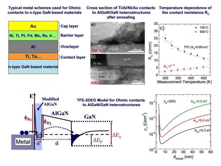
- MOS systems on GaN and SiC and other wide band gap semiconductors
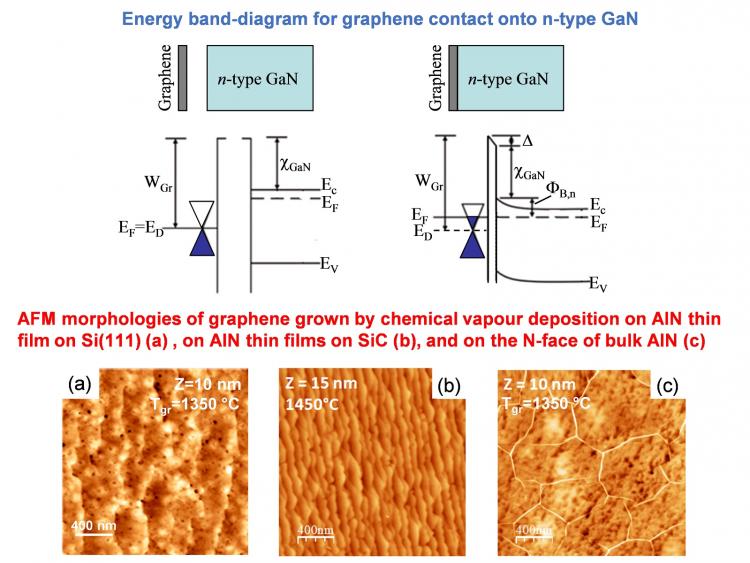
- Dielectrics on 2D materials: metal dichalcogenides (MoS2, WSe2, MoSe2 etc) and on Graphene
- Theory and modeling: growth of dielectrics by ALD, MOCVD, PLD, MBE, etc.; interfaces, 2D materials, circuit implications; Simulations and modeling of breakdown, reliability, trapping etc.
- Characterization methods with high sensitivity & spatial resolution; SOI and GOI wafer engineering;
- SiO2 and oxynitrides (growth, characterization, reliability, radiation effects and applications); Reliability, Variability, electrical and physical characterization methods of classical and alternative dielectrics on single or multi-layered 2D systems
- Emerging dielectric materials and technologies: oxide/semiconductor interfaces in solar cells; Dielectrics for capacitors, MEMS and sensors applications; Light emission from dielectrics, Si/SiO2 superlattices, nanoclusters embedded in dielectrics; Dielectrics for TFTs, amorphous or organic devices; MOS structures in rectennas and water splitting cells
On the high-k / III-V topic at WoDiM 2016 there was a joint workshop with the EU Research Project COMPOSE3 (http://www.zurich.ibm.com/news/14/compose3.html).
INVITED SPEAKERS: Christopher Hinkle, UTDallas; Gaudenzio Meneghesso, Padua Univ.; James H. Stathis, IBM-USA; Jacopo Franco, IMEC; Nava Setter, EPFL; Christian Wenger, IHP; Barbara De Salvo, LETI; Hiroshi Iwai, Tokyo IoT; Erik Lind, Lund Univ.; Alain Bravaix, IM2NP; Moshe Eizenberg, Technion, Thierry Baron, CNRS; Vladimir Djara, IBM-Switzerland
Chair
Salvatore Lombardo,
Web Site: http://wodim2016.imm.cnr.it
WoDiM Committee: Anton Bauer, Volkhard Beyer; Mikael Cassé; Karim Cherkaoui; Catherine Dubourdieu; Karol Fröhlich; Blas Garrido Fernandez; Gérard Ghibaudo; Gabriella Ghidini; Paul Hurley; Fernanda Irrera; Ben Kaczer, Salvatore A. Lombardo, Montserrat Nafría Maqueda; Andreas Martin; Alessandro Paccagnella; Thomas Schroeder; Chadwin Young